-
电路设计 > eMMC应用和PCB layout布局布线参考设计
目录
eMMC介绍
主要针对现在主流的eMMC5.0以及以上版本。
eMMC信号大体介绍
如下表格:
Pin Name
Type
Description
中文描述
DAT0 - DAT7
I/O
Bidirectional data channels used for data transfers.
用于数据传输的双向数据通道。
CMD
I/O
Bidirectional command channel used for device initialization and command transfers.
用于设备初始化和命令传输的双向命令通道。
CLK
Input
Clock input.
时钟输入
RST_N
Input
Hardware reset.
硬件复位
VCC
Power
Supply voltage for the flash memory.
闪存的电源电压。
VCCQ
Power
Supply voltage for the memory controller and MMC interface.
存储器控制器和MMC接口的电源电压。
VDDI
Power
Internal power node. Connect capacitor to ground.
内部电源节点。将电容器接地。
VSS
Power
Ground pin for the flash memory.
闪存的接地针脚。
VSSQ
Power
Ground pin for the memory controller and MMC interface.
内存控制器和MMC接口的接地引脚。
DS
Output
Data Strobe.
数据选通。
NC
—
Not connected.
未连接
RFU
—
Reserved for future use. Do not connect.
预留为将来使用
EMMC4.5和5.0封装和兼容性对比
如下:
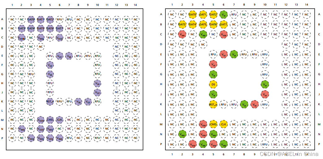
Ball
e·MMC 4.51
e·MMC 5.0
Comment
H5
RFU
DS
DS can be floating if HS400 is not used.
A6, J5
RFU
VSS
VSS can be floating if HS400 is not used.
C5
RFU
NC
Used for routing in this technical note only
because it is NC internally, and JEDEC rede
fined it as NC for e·MMC 5.0.
EMMC5.0和5.1封装和兼容性对比
如下:
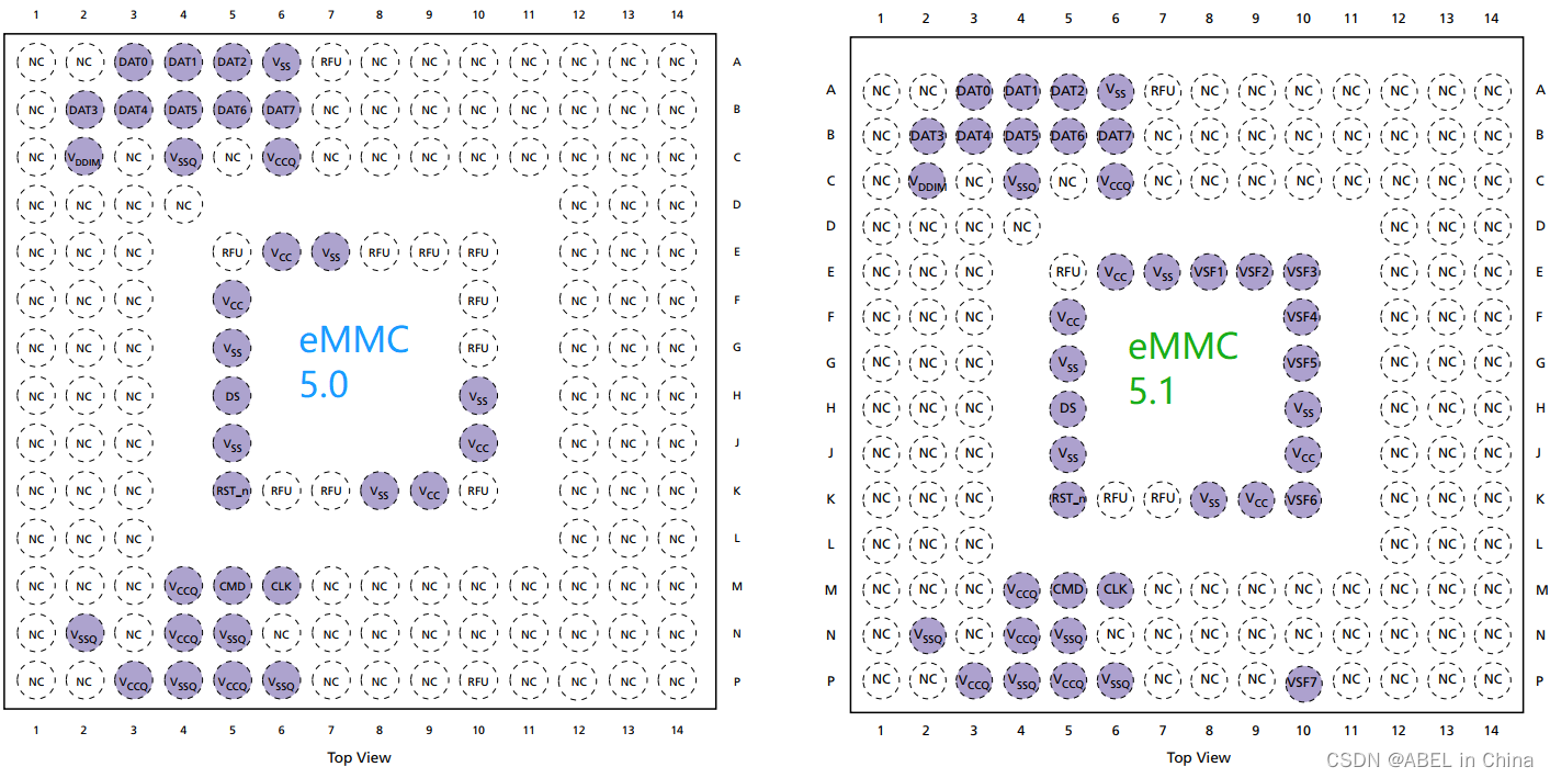
之前版本eMMC版本中的一些RFU球在e.MMC 5.1中变为VSF,153pin:E8、E9、E10、F10、G10、K10、P10。VSF球用于系统内分析和调试;其功能在中禁用,只有厂家可以通过特殊测试固件和安全主机认证。良好的做法是将VSF球暴露在测试点上;否则,请保持它们未连接。
PCB Layout建议
关于eMMC5.1版本的PCB走线layout和滤波电容摆放建议如下:


Recommended decoupling capacitors:
— VCCQ ≥ 0.1 uF x1 and 2.2 uF x1 (this cap should be as close as possible to the C6 ball) and 1 x 1uF
— VCC ≥ 0.1uF x1 and 2.2uF x1
— VDDI ≥ 0.1uF x1 and 2.2uF x1
原理图参考设计如下:
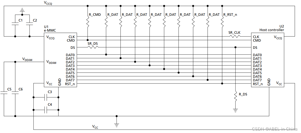
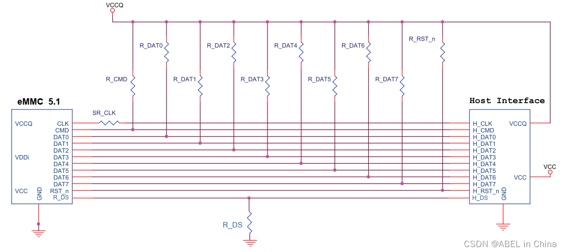
Parameter
Symbol
Recommended
Comments
Pull-up resistance for CMD
R_CMD
10 k
To prevent bus floating.
Pull-up resistance for DAT[7:0]
R_DAT
50 k
To prevent bus floating.
Pull-up resistance for RST_n
R_RST_n
50 k
A pull-up resistance on the RST_n (H/W reset) line is
not required if the host does not enable the H/W reset
feature.
Series termination for CLK
SR_CLK
22
To stabilize the clock signal. It is recommend for
customers to perform simulations using the controller
IBIS model to confirm this value.
Pull-Down resistance for Data
Strobe
R_DS
50 k
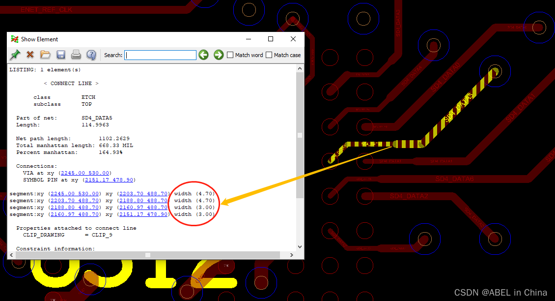
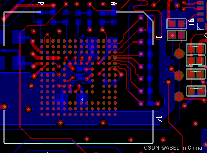
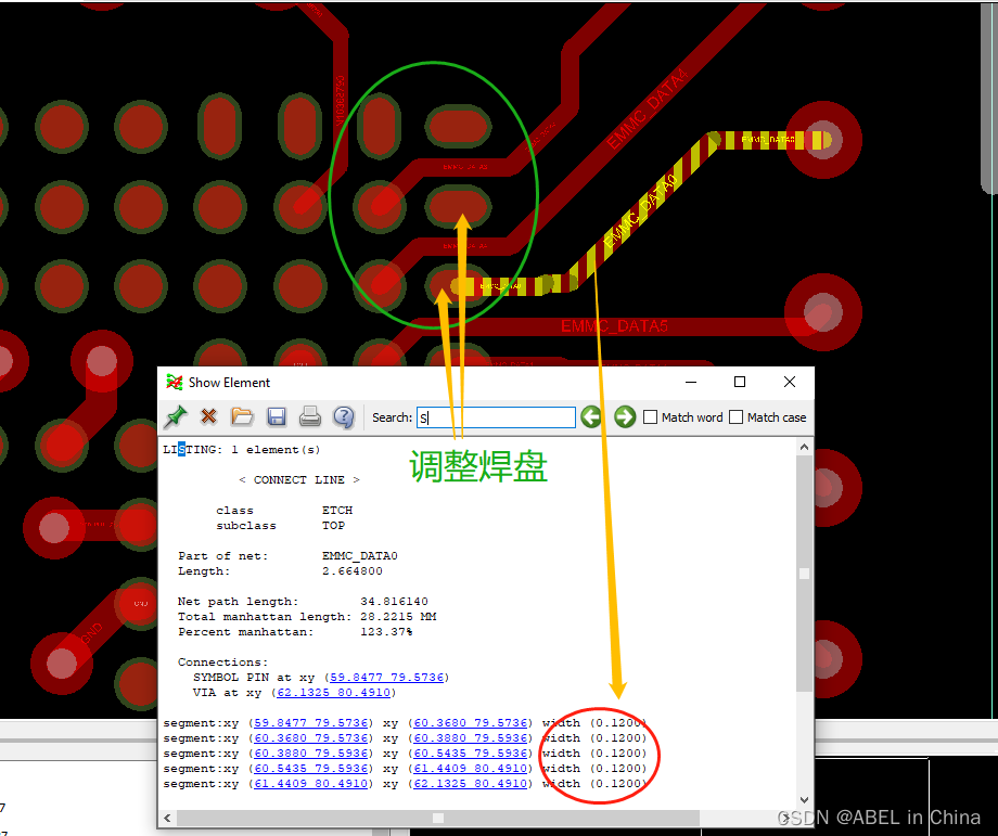
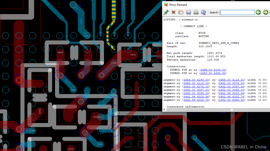
PCB layout参考设计
参考设计1


参考设计2

参考设计3
参考设计4
参考设计5
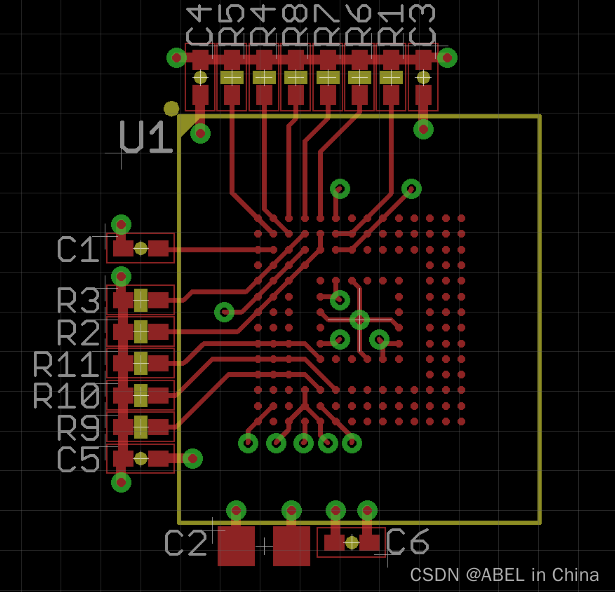
前面的参考设计显示了v5.x eMMC设备使用大致6mil宽度布线和12mil/24mil过孔的示例布线。需要注意的一点是,由于eMMC球的间距,可能需要调整线宽,以使线可以通过“NC”球。
从参考设计1-4都采用了为了躲避NC进行线缆的粗细调整,参考设计5采用直接穿过NC PIN的layout方式,关于参考设计5,从厂家给的建议如下:

e·MMC signals can be fanned out through NC pins. No internal connection is present for NC pins. Micron recommends that e·MMC signals not be fanned out through RFU pins.
e·MMC信号可以通过NC引脚扇出。NC引脚不存在内部连接。Micron建议不要通过RFU引脚扇出e·MMC信号。
大家可以根据自己的认识对eMMC进行pcb layout,此文章只是作为参考。enjoy it
抖动的声音:dilo_Abel
-
相关阅读:
【转】大数据安全--敏感数据识别和分级打标
外贸新手如何利用领英寻找你的潜在客户(建议收藏)
精品SpringCloud商品服务系统微服务分布式疫情下购物商城
H3C构建中小型企业网络(NE)
Linux——Linux用户管理、组管理和文件管理常用命令总结
基于粒子群优化和模拟退火算法增强传统聚类研究(Matlab代码实现)
vue3 搭配ElementPlus做基础表单校验 自定义表单校验
Leetcode 231.2的幂
还有人不知道这个电商软件?
7、架构-架构的安全性
- 原文地址:https://blog.csdn.net/DL_62532/article/details/128087537