-
ADS Circuit Design Cookbook
文章目录
- Getting Started
- Tuning and Optimization
- Harmonic Balance
- Planar EM Simulation
- Using FEM Simulator
- RF System Design
- Microwave Discrete and Microstrip Filter Design
- Discrete and Microstrip Coupler Design
- Microstrip and CPW Power Divider Design
- Microwave Amplifier Design
- Monte Carlo and Yield Analysis
- MESFET Frequency Multiplier Design
- Active Mixer Design
- 1GHz VCO Design
- Power Amplifier Design
- Design of RF MEMS Switches
- Getting Started with ADS Ptolemy
- QPSK System Design using ADS Ptolemy
- DSP / RF Co-simulation
- Antenna Pattern with Circuit Components
- How to perform Deembedding
- How to use Vendor Component Libraries
Getting Started
Step 1 - Creating Workspace
1.File > New > Workspace
2.Select the libraries to be included in the workspace

3.Provide the library name under which user would like to organize the work.
4.Select the preferred units to be used during the design.Step 2 - Creating Schematic Design
File >New >Schematic
Tuning and Optimization
It is often the case that our manually calculated values do not provide the most optimum performance and it is needed to change the component values. This can be done in two ways: Tuning or Optimization.
What is Tuning?
Tuning is a way in which we can change the component values and see the impact of the same on circuit performance. This is a manual way of achieving the required performance from a circuit which works well in certain cases
What is Optimization?
Optimization is an automated procedure of achieving the circuit performance in which ADS can modify the circuit component values in order to meet the specific optimization goals. Please note that
care should be taken while setting up the goals to be achieved and it should be practically possible else it will not be possible to meet the goals. Also the component values which are being optimized
should be within the practical limits and this needs to be decided by designers considering the practical limitations.

Performing Tuning
1.选择【tuning】控件,然后选择相关的器件,然后上下拉相关的器件参数,直到指标满足要求为止;
2.Once we have achieved the desired or best possible results we can click Update Schematic button to update these tuning values on design schematic.


Performing Optimization
- Setting up Optimization Goals
- Placing Optimization Controller and select type of optimizer and number of iterations
- Make component values optimization ready


Defining Component Values to be Optimization ready


- Go to Simulate->Simulation Variables Setup.
- Click Optimization Tab in the variable setup window (this variable window is a single place where we define components to be tunable, optimization or set their tolerances for Statistical analysis)
- Select all the “L” and “C” values to Optimize and set their min and max as per your own convenience (make sure that the value limits are realistic).


最后update结果,得到的数据如下:

Harmonic Balance
Harmonic balance is a frequency-domain analysis technique for simulating distortion in nonlinear circuits and systems. It is well-suited for simulating analog RF and microwave problems, since these are most naturally handled in the frequency domain. You can analyze power amplifiers, frequency multipliers, mixers, and modulators etc., under large-signal sinusoidal drive.
Harmonic balance simulation enables the multi-tone simulation of circuits that exhibit inter-modulation frequency conversion. This includes frequency conversion between harmonics. Not only can the
circuit itself produce harmonics, but each signal source (stimulus) can also produce harmonics or small-signal sidebands. The stimulus can consist of up to 12 non-harmonically related sources. The total number of frequencies in the system is limited only by such practical considerations as memory, swap space, and simulation speed.
The harmonic balance method is iterative. It is based on the assumption that for a given sinusoidal excitation there exist steady-state solutions that can be approximated to satisfactory accuracy by
means of a finite Fourier series. Consequently, the circuit node voltages take on a set of amplitudes and phases for all frequency components. The currents flowing from nodes into linear elements,
including all distributed elements, are calculated by means of a straightforward frequency-domain linear analysis. Currents from nodes into nonlinear elements are calculated in the time-domain.
Generalized Fourier analysis is used to transform from the time-domain to the frequency-domain.
The Harmonic Balance solution is approximated by truncated Fourier series and this method is inherently incapable of representing transient behavior. The time-derivative can be computed exactly
with boundary conditions, v(0)=v(t), automatically satisfied for all iterates.
The truncated Fourier approximation + N circuit equations results in a residual function that is minimized.
N x M nonlinear algebraic equations are solved for the Fourier coefficients using Newton’s method and the inner linear problem is solved by:
• Direct method (Gaussian elimination) for small problems.
• Krylov-subspace method (e.g. GMRES) for larger problems.
Nonlinear devices (transistors, diodes, etc.) in Harmonic Balance are evaluated (sampled) in the timedomain and converted to frequency-domain via the FFT.

单音信号谐波分析

TOI=20,输入信号为-20dBm时候,输出的谐波情况如下图:

TOI=20,输入信号为-10dBm时候,输出的谐波情况如下图:

从如上两个图可以看出,输入信号减小10dB,输出信号减小了30dB;输入信号扫频
建立原理图;

【parameter sweep】控件输入如下扫频计划和仿真的控件;

得到的输出结果;

增加方程,查看增益的情况,方程如果有错误,会显示为红色;


查看一阶和三阶的扫描情况;

Planar EM Simulation
Agilent ADS provides two key electromagnetic simulators integrated within its environment making it convenient for the designers to perform EM simulations on their designs. Unlike circuit simulators, EM
simulators are used on layout.Microstrip Bandpass Filter

Creating the Schematic Design for BPF
创建原理图;

查看结果;

Creating the Layout from Schematic
将创建好的原理图导入到ADS layout中;


Setup and run EM simulation
To run EM simulation it is need to setup the required things properly.

选择【EM】控件,将下图中的各个选项设置好;
Substrate设置,port端口设置,frequency plan设置,设置好后点击保存;


同时在option选项中,选中edge mesh;

选设置好后,保存,然后点击仿真;


Comparison of EM and Schematic Results
In order to see both the results on the same graph, double-click the Momentum graph and click the drop down list to locate the dataset for the circuit. It should be with the same name as the cell name (e.g. Lab4_Mstrip_Filter) and select S(1,1) and S(2,1) in dB. observe the response with both circuit simulation as well as Momentum simulation
response to compare their performance.

Patch Antenna Design
A microstrip antenna in its simplest configuration consists of a radiating patch on one side of a dielectric substrate, which has a ground plane on the other side. The patch conductors usually made
of copper or gold can be virtually assumed to be of any shape. However, conventional shapes are normally used to simplify analysis and performance prediction. The radiating elements and the feed lines are usually photo etched on the dielectric substrate.The radiating patch may be square, rectangular, circular elliptical or any other configuration. Square, rectangular and circular shapes are the most common because of ease of analysis and fabrication.
Some of the advantages of the microstrip antennas compared to conventional microwave antennas are:
• Low weight, low volume
• Low fabrication cost
• Easy mass production
• Linear and circular polarization are possible with simple feed
• Easily integrated with MIC
• Feed lines and matching networks can be fabricated simultaneously with antenna structures
Patch antennas find various applications stating from military to commercial, because of their ease of design and fabrication. Patch arrays are extensively used in phased array radar applications and in
applications requiring high directivity and narrow beam width.Calculating Patch Antenna Dimensions
- Select an appropriate substrate of thickness (h) and dielectric constant (εr) for the design of the patch antenna. In present case, we shall use following Dielectric for design:
a. Height: 1.6 mm
b. Metal Thickness: 0.7 mil (1/2 oz. Copper)
c. Er: 4.6
d. TanD: 0.001
e. Conductivity: 5.8E7 S/m - Calculate the physical parameters of the patch antenna as shown in the geometry in the following illustration using the given formula.

The width and length of the radiating surface is given by,

where,
• Velocity of light c = 3 X 10⁸ m/s2
• Frequency, f = 2.4 GHz
• Relative Permittivity εr = 4.6
The depth of the feed line in to the patch is given by: H=0.822*L/2 = 12 mm
The other dimensions are,
• Y= W/5 = 5.8 mm
• X = Z = 2W/5 = 11.7 mm
Creating Patch Antenna Geometry
1.创建天线形状,选择【insert】→【pylon】;

2.给天线添加port1;

3.单击【EM】控件,设置相关参数;


Antenna Simulation
保存好相关参数后,进行仿真;

仿真结束后,查看结果;

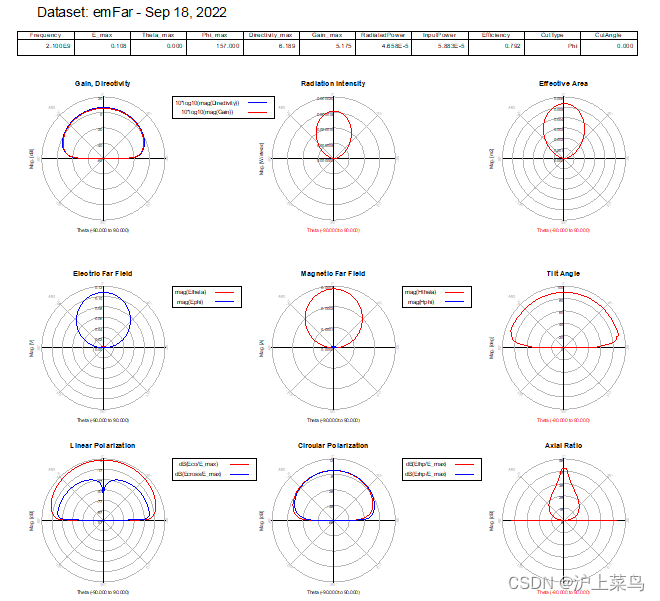
Antenna Radiation Pattern
-
For Far-Field Antenna Pattern, go to EM > Post Processing > Far Field and select the desired frequency (e.g. 2.4 GHz) and click Compute.

之后出现了一个错误,如下图所示,解决的方法为下图,将【save current for】中选为all generated frequency即可;


-
Far field computation will be done and results will be displayed in the post processing window as shown below. We can use Window >Tile and then go to Plot Properties (from the bottom tabs) and then select Far Field >Antenna Parameters to see all the required data.


-
Go to Far Field Cut tab and select the Phi and click Display Cut in data display button

EM / Circuit Co-simulation
What is EM / Circuit co-simulation?
Often there is a requirement of having discrete components such as R, L, C, Transistor, Diodes etc in the layout but EM solvers cannot simulate these discrete components directly hence we use Co-simulation whereby we create a layout component and then place it into the schematic for assembly of discrete components.
Typical process for EM/Circuit co-simulation
- Connect Pins in the layout where we need to make connections for discrete components
- Define the stackup and other regular EM settings like Mesh, Simulation Frequency range etc.
- Create an EM Model and Symbol for this layout component
- Place this layout component in Schematic and connect the required discrete components
- Set up the appropriate simulation in schematic. Momentum/FEM simulation will be performed if it is already not done else the same data will be reused.
Create a layout where co-simulation needs to be performed
- Create layout manually or generate it from the schematic as described in earlier sections.
- Place Pins wherever we need to make connections or assemble discrete parts alongwith layout
- In this case we have used “cond” layer for conductors and “hole” layer for VIA to provide a path to ground.

- Create a substrate with 25 mil Alumina substrate having Er=9.9, TanD=0.0009 and cond layer as Gold with conductivity of 4.1E7 and thickness of 0.7 mil. “hole” layer mapped as VIA will also have Gold conductivity as shown in graphics.
- Setup the frequency plan as needed for schematic simulation
1)创建layout;

2)过孔的添加方法;


具体参考:
https://blog.csdn.net/weixin_39861362/article/details/86109805
https://blog.csdn.net/weixin_39861362/article/details/86192701
3)添加port;
Create EM / Circuit co-simulation component and symbol
点击EM控件,设置相关的板材参数、频率参数、mesh设置,点击go则生成emCosim文档(包含emModel和symbol);


Simulation and database generation process
1)新建原理图,将enCosim模型添加到原理图中;

2)进行仿真,得到结果;

Using FEM Simulator
Introduction
FEM simulator provides a complete solution for electromagnetic simulation of arbitrarily-shaped and passive three-dimensional structures. FEM simulators create full 3D EM simulation an attractive option for designers working with RF circuits, MMICs, PC boards, modules, and Signal Integrity applications. It provides fully automated meshing and convergence capabilities for modeling arbitrary 3D shapes such as bond wires and finite dielectric substrates. Along with Momentum, FEM simulator in ADS provide RF and microwave engineers access to some of the most comprehensive EM simulation tools in the industry.
Developed with the designer of high-frequency/high-speed circuits in mind, FEM Simulator offers a powerful finite-element EM simulator that solves a wide array of applications with impressive accuracy and speed.The Finite Element Method
To generate an electromagnetic field solution from which S-parameters can be computed, FEM Simulator employs the finite element method. In general, the finite element method divides the full problem space into thousands of smaller regions and represents the field in each sub-region (element) with a local function.
In FEM Simulator, the geometric model is automatically divided into a large number of tetrahedra, where a single tetrahedron is formed by four equilateral triangles.Representation of a Field Quantity
The value of a vector field quantity (such as the H-field or the E-field) at points inside each tetrahedron is interpolated from the vertices of the tetrahedron. At each vertex, FEM Simulator stores the components of the field that are tangential to the three edges of the tetrahedron. In addition, the component of the vector field at the midpoint of selected edges that is tangential to a face and normal to the edge can also be stored. The field inside each tetrahedron is interpolated from these nodal values.
Basis Functions
A first-order tangential element basis function interpolates field values from both nodal values at vertices and on edges. First-order tangential elements have 20 unknowns per tetrahedra.
Size of Mesh vs. Accuracy
There is a trade-off between the size of the mesh, the desired level of accuracy, and the amount of available computing resources.
On one hand, the accuracy of the solution depends on the number of the individual elements (tetrahedra) present. Solutions based on meshes that use a large number of elements are more accurate than solutions based on coarse meshes using relatively few elements. To generate a precise description of a field quantity, each tetrahedron must occupy a region that is small enough for the field to be adequately interpolated from the nodal values.
However, generating a field solution for meshes with a large number of elements requires a significant amount of computing power and memory. Therefore, it is desirable to use a mesh that is fine enough to obtain an accurate field solution but not so fine that it overwhelms the available computer memory and processing power.
To produce the optimal mesh, FEM Simulator uses an iterative process in which the mesh is automatically refined in critical regions. First, it generates a solution based on a coarse initial mesh. Then, it refines the mesh based on suitable error criteria and generates a new solution. When selected, S-parameters converge to within a desired limit, the iteration process ends.Field Solutions
During the iterative solution process, the S-parameters typically stabilize before the full field solution. Therefore, when analyzing the field solution associated with a structure, it may be desirable to use a convergence criterion that is tighter than usual.
In addition, for any given number of adaptive iterations, the magnetic field (H-field) is less accurate than the solution for the electric field (E-field) because the H-field is computed from the E-field using the following relationship:

Thus, making the polynomial interpolation function an order lower than those used for the electric field.Implementation Overview
To calculate the S-matrix associated with a structure, the following steps are performed:
- The structure is divided into a finite element mesh.
- The waves on each port of the structure that are supported by a transmission line having the same cross section as the port are computed.
- The full electromagnetic field pattern inside the structure is computed, assuming that each of the ports is excited by one of the waves.
- The generalized S-matrix is computed from the amount of reflection and transmission that occurs.
The final result is an S-matrix that allows the magnitude of transmitted and reflected signals to be computed directly from a given set of input signals, reducing the full three-dimensional electromagnetic behavior of a structure to a set of high frequency circuit values.
Setting up FEM Simulation
Key steps to be followed for a successful FEM simulation in ADS are:
- Creating a Physical design
- Defining Substrates
- FEM Simulation Setup:
a. Assigning Port Properties
b. Defining Frequency and output plan
c. Defining Simulation Options e.g. Meshing, Solver Selection (Direct or Iterative) etc.
d. Run FEM Simulation - View the Results, Far Fields etc.
Microstrip Low Pass Filter
1)建模;

2)设置板材;

3)设置端口和output plan及options;


4)仿真,生成数据;

5)可视化查看数据;


Symmetry Planes in FEM
To reduce the size of the problem and memory requirement for faster simulations, FEM simulator in ADS can utilize the symmetric boundary condition either in E-plane or H-plane so that only half of the structure is simulated thus requiring lesser system resources.
Adding a Symmetry Plane
A symmetry plane defines the boundary on one side of the circuit substrate. Only one box, or a waveguide, or a symmetry plane can be applied to a circuit at a time. When a symmetry plane is defined, the simulation results will be equivalent to the results of a larger circuit that would be created by mirroring the circuit about the symmetry plane.
For symmetric circuits, this enables faster simulations that require less memory because only half the actual structure needs to be simulated.
To add a symmetry plane:- Choose EM > FEM Symmetry Plane > Add Symmetry Plane.
- Select the direction of the symmetry plane. To insert the symmetry plane parallel to the x-axis, click X-axis. To insert the symmetry plane parallel to the y-axis, click Y-axis.
- Insert the symmetry plane using one of the following two methods:
a. Position the mouse and click to define the location of the symmetry plane.
b. From the Layout menu bar, select Insert > Coordinate Entry and use the Coordinate
Entry X and Coordinate Entry Y fields to specify a point on the edge of the substrate. - Click Apply.
Editing a Symmetry Plane
Once the symmetry plane is applied, you cannot change its location. If you want to change the location or orientation, you must delete the current symmetry plane and add a new one.
Deleting a Symmetry Plane
To delete a symmetry plane:Select EM > FEM Symmetry Plane> Delete Symmetry Plane. The symmetry plane is removed from the layout.
总结
Step 1 - Create partial design
Step 2 - Applying Symmetry Plane
Step 3 - FEM SimulationRF System Design
Receiver System Design
1)创建原理图;

2)查看仿真结果;


Phase Noise Simulation
1)原理图绘制;

2)结果查看;

2-Tone Simulation of Receiver System
1)绘制原理图;

2)查看结果数据;

RF System Budget Analysis
Performing RF System Budget is very useful to characterize the system behavior and analyze how system behaves as the signal transitions from each component. Easiest way to perform RF System Budget analysis is using Budget Controller which offers more than 40 built-in budget measurements offering great ease-of-use.
One of the fundamental rules to follow while using Budget Controller is that system should only have 2-port components with exception of S2P files, AGC Amplifier with Power Control. ADS SimulationBudget library provides special Mixer with Internal LO so that super-heterodyne type of systems can be analyzed.
1)创建原理图;

2)查看结果;


Microwave Discrete and Microstrip Filter Design
Theory
Microwave filters play an important role in any RF front ends for the suppression of out of band signals. They in the lumped and distributed form are extensively used for both commercial and military applications. A filter is reactive network that passes desired band of frequencies while almost stops all other band of frequencies. The frequency that separates the transmission band from the attenuation band is called the cut-off frequency and denoted as fc. The attenuation of the filter is denoted in decibels or nepers. A filter in general can have any number of pass bands separated by stop bands. They are mainly classified in to four common types namely lowpass, highpass, bandpass and band stop filters.
An ideal filter should have zero insertion loss in the pass band, infinite attenuation in the stop band and a linear phase response in the pass band. Ideal filter cannot be realizable as the response of an ideal low pass or band pass filter is rectangular pulse in frequency domain. When converting this rectangular pulse into time domain results in sinc function which makes the filter system to be causal. Hence ideal filter is not realizable hence the art of filter design necessitates compromises with respect to cutoff and roll off. There are basically three methods for filter synthesis. They are Image parameter method, Insertion loss method and numerical synthesis. The image parameter method is an old and crude method whereas the numerical method of synthesis is novel but cumbersome. The insertion loss method of filter design on the other hand is the optimum and more popular method for higher frequency applications. The filter design flow for insertion loss method is shown in figure below.

Since characteristics of an ideal filter cannot be obtained, the goal of filter design is to approximate the ideal requirements within an acceptable tolerance. There are four types of approximations namely Butterworth or maximally flat, Chebyshev, Bessel and Elliptic approximations. For the proto type filters, maximally flat or Butterworth provides the flattest pass band response for a given filter order. In the Chebyshev method, sharper cutoff is achieved and the pass band response will have ripples of amplitude 1+k2.
Bessel approximations are based on the Bessel function which provides sharper cutoff and Elliptic approximations results in pass band and stop band ripples. Depending on applications and the cost the approximations can be chosen. The optimum filter is Chebyshev filter with respect to response and the bill of materials. Filter can be designed both in the lumped and distributed form using the above approximations.Design of Microwave Filters
The first step in the design of Microwave filter is to select a suitable approximation of the prototype model based on the specifications.Calculate the order of the filter from the necessary roll off as per the given specifications. The order can be calculated as follows


Lumped and Distributed Lowpass filter Simulation


Schematic Simulation steps for Lumped Low Pass Filter


Layout Simulation steps for Distributed Low Pass Filter
Calculate the physical parameters of the distributed lowpass filter using the design procedure given above. Calculate the width of the Zl and Zh transmission lines for the design of the stepped impedance lowpass filter. In this case Zl = 10Ω and Zh = 100Ω and the corresponding line widths are 24.7 mm and 0.66mm respectively for a dielectric constant of 4.6 and a thickness of 1.6 mm
1)创建PCB图,根据ADS中【TOOL】→【Lincal】,计算微带线的长度和宽度,对于50Ohm的trace可以很简单计算出长和宽,串联电感和并联电容转化为微带线的方法详见下列两个链接;

https://blog.csdn.net/rzchong1988/article/details/113591915
https://blog.csdn.net/rzchong1988/article/details/1136153782)绘制好微带滤波器的尺寸,添加好端口,然后点击【EM】控件,设置好频率,将option控件中的edge mesh打开,然后点击仿真,查看结果;


It can be noted that 3dB cut-off has shifted to 1.61GHz instead of 2 GHz as our theoretical
calculations doesn’t allow accurate analysis of open end effect and sudden impedance change of the transmission lines hence the lengths of the lines needs to optimized little bit to recover the desired 2GHz cutoff frequency specifications.This optimization can be carried out using Momentum simulator in ADS or by performing parametric sweep on the lengths of Capacitive and Inductive lines.Parametric EM simulations
1)To begin parametric simulation on the layout, we need to define the variable parameters which shall be associated with the layout components. Click EM > Component > Parameters as shown below
定义微带线的长度变量;

添加了变量之后,相应的要把layout中的各个值修改为变量的形式,如下图:

2)After defining all the parameter values in the desired layout components we can create an EM model and symbol which shall then be used for parametric EM cosimulation in schematic. To create a parametric model and symbol for the layout, click “EM > Component > Create EM Model and Symbol” option.


3)新建一个原理图,把刚刚生成的emModel拖拽到新的原理图中,


2)仿真,查看结果(结果不正确,为什么无法输出一系列的多组曲线簇)
Discrete and Microstrip Coupler Design
Theory
A coupler is basically a device that couples the power from the input port to two or more output ports equally with less loss and with or without the phase difference. The branch line coupler is a 3 dB coupler with 900-phase difference between the two output ports. An ideal branch line coupler as shown in figure 1 is a four-port network and is perfectly matched at all the four ports.

The power entering in port 1 is evenly divided between ports 2 and 3, with a phase shift of 90 degree between the ports. The 4th port is the isolated port and no power flows through it. The branch line coupler has a high degree of symmetry and allows any of the four ports to be used as the input port.
The output ports are in the opposite sides of the input port and the isolated port is in the same side of the input port. This symmetry is reflected in the S matrix as each row can be the transposition of the first row. The [S] matrix of the ideal branch line coupler is given as follows
The major advantage of this coupler is easier realization and disadvantages are lesser bandwidth due to the use of quarter wave length transmission line for realization and discontinuities occurring at the junction. To circumvent the above disadvantages multi sections of branch line coupler in cascade can increase the bandwidth by a decade and 10° – 20° increase in length of the shunt arm can compensate the power loss due to discontinuity effects.Design a lumped element and distributed branch line coupler at 2 GHz


1)设计原理图;

2)仿真查看结果

Distributed Branch Line Coupler Design
- Select an appropriate substrate of thickness (h) and dielectric constant (εr) for the design of
the coupler. For present example, we will select following dielectric parameters:
a. Er = 4.6
b. Height = 1.6 mm
c. Loss Tangent = 0.0023
d. Metal Thickness = 0.035 mm
e. Metal Conductivity = 5.8E7 S/m - Calculate the wavelength λg from the given frequency specifications as follows

- Synthesize the physical parameters (length & width) for the λ/4 lines with impedances of Z0and Z0/ 2 (Z0 is the characteristic impedance of microstrip line is which taken as 50Ω). The geometry of the Branch line coupler is shown in figure below.

创建layout,设置板材及常数;
功分器有两种阻抗:50ohm和35ohm,根据ADS中自带的微带线长度宽度计算软件,得出其相应的长和宽分别为:


4)仿真,查看结果,如果结果不理想可以调节TL5和TL6的臂长,直到结果满意为止;

Microstrip and CPW Power Divider Design
Theory
A power divider is a three-port microwave device that is used for power division or power combining. In an ideal power divider the power given in port 1 is equally split between the two output ports for power division and vice versa for power combining as shown below. Power divider finds applications in coherent power splitting of local oscillator power, antenna feedback network of phased array radars, external leveling and radio measurements, power combining of multiple input signals and power combining of high power amplifiers.

T-Junction Power Divider
The different types of power divider are T junction power divider, Resistive divider and Wilkinson power and hybrid couplers. The T –junction power divider is a simple 3-port network and can be implemented in any kind of transmission medium like microstrip, stripline, coplanar wave guide etc. Since, any 3-port network cannot be lossless, reciprocal and matched at all the ports, the T junction power divider being lossless and reciprocal cannot be perfectly matched at all the ports. The T junction power divider can be modeled as a junction of three transmission lines as shown in figure below.

Distributed T junction Power Divider(3GHz)

1)选择板材,设置介电常数,计算50ohm和70.7ohm阻抗线的长度和宽度;

2)绘制layout,进行仿真;

3)查看结果;

Wilkinson Power Divider
The Wilkinson power divider is robust power divider with all the output ports matched and only the
reflected power is dissipated. The Wilkinson power divider provides better isolation between the
output ports when compared to the T junction power divider The Wilkinson power divider can also be
used to provide arbitrary power division. The geometry of Wilkinson power divider and its
transmission line equivalent is shown in figure below

Lumped model Wilkinson Power divider(3GHz)

1)创建原理图;

2)仿真,查看结果;

Distributed Wilkinson power divider

1)设置板材及相关常数,计算50ohm和70.7ohm阻抗下的线宽和线长;

2)设置端口,频率,生成emCosimu文档;

3)新建一个原理图,将emModel插入,并插入电阻100ohm;

4)仿真,查看结果;

CPW T junction power divider
Design Procedure

1)板材选择,计算50ohm和70.7ohm下的线宽、线长以及gap;


2)绘制layout,选择【Tline-waveguide】控件,然后选择CPW(未完待续);

Microwave Amplifier Design
Introduction
Amplifier is integral part of any communication system. The purpose of having an amplifier in a system is to boost the signal to the desired level. It also helps in keeping the signal well above noise so that it could be analyzed easily and accurately. Choice of amplifier topology is dependent on the individual system requirements and they could be designed for Low Frequency applications, medium to high frequency applications, mm-wave applications etc. and depending upon the system in which they are used, amplifiers can adopt many design topologies and could be used at different stages of system and accordingly they are classified as Low Noise Amplifiers, Medium Power Amplifiers, and
Power Amplifiers etc. The most common structure that still finds application in many systems tends to be a Hybrid MIC amplifier. The main design concepts for amplifiers regardless of frequency and system remain the same and they need to be understood very clearly by a designer. Specific frequency ranges pose their own unique design challenges and needed to taken care by designers appropriately. This paper focuses on design of a small signal C-band Hybrid MIC amplifier. This procedure is equally valid for other amplifiers operating in other frequency ranges with minor changes in the design procedure.Amplifier Theory
There are few things that need to be understood by designer before he can start designing amplifiers like stability and matching conditions. These are discussed in the section below, there are many references available on amplifier basic concept and design procedure, the formula presented in this paper are taken from one of them.
Stability Condition
Stability analysis is the first step in any amplifier design. The stability of an amplifier or its resistance to oscillate is an important consideration in a design and can be determined from S-parameters, the matching networks, and the terminations. In a two-port network, oscillations are possible when either

Matching Conditions
Amplifier could be matched for variety of conditions like Low Noise applications, unilateral case and bilateral case. The formulae for each condition are given below for designer’s knowledge.
Optimum Noise Match
The matching for lowest possible noise figure over a band of frequencies require that particular source impedance be presented to the input of the transistor. The noise optimizing source impedance is called as Γopt, and is obtained from the manufacturers data sheet. The corresponding load impedance is obtained from the cascade load impedance formula.

Unilateral Case

Bilateral Case (when S12≠0)

The common source configuration is normally chosen for the highest gain per stage. If the stability factor K>1, the network gives MAG. If K<1, the network could cause oscillations i.e. Gmax is infinite and given as

This should be avoided by locating the region of instability in ΓS and ΓL planes.CAD oriented design procedure
The CAD oriented design procedure consists of following steps, which will be described one by one for reference and understanding of the designers.
- DC Analysis
- Bias circuit design
- Stability analysis
- Input and Output matching network design
- Overall Amplifier performance optimization
Amplifier Specifications
• Frequency Band: 5.3 GHz – 5.5 GHz
• Gain: 12 dB or more
• Gain Flatness: +/- 0.25 dB (max.)
• Input/Output Return Loss: < -15 dB
• DC Power Consumption: 50 mW (max.)DC Analysis
Bias network design
Bias network design for amplifier is dependent on the frequency range in which amplifier needs to be designed, that is to say if amplifier needs to be design for low frequency application then a choke (inductor) is used but getting discrete inductors at microwave frequencies is difficult so high impedance quarter wavelength line (λ/4) at center frequency is the best possible choice which designers can choose to design bias network. The thing that needs to be noted in bias circuit design is that more often than not this λ/4 is followed by a resistor or a bypass capacitor and these components adds extra length to the λ/4 line which designers sometime neglect and this could cause some desired RF frequency power to be dissipated in this branch which affects the gain and
frequency response of the amplifier, so this calculated λ/4 line needs to adjusted by taking proper care of these extra elements and their footprints. One probable and commonly used method is to use Radial stub immediately after λ/4 high impedance bias line which will help to achieve proper isolation at desired RF frequency, no matter what component is added after λ/4 long bias line.
Schematic illustration below shows the circuit design for bias circuit where it could be seen that high impedance λ/4 bias line is immediately followed by a Radial stub and then by a resistor and capacitor to ground. For more illustration layout of the bias network is shown.

Monte Carlo and Yield Analysis
MESFET Frequency Multiplier Design
Active Mixer Design
1GHz VCO Design
Power Amplifier Design
Design of RF MEMS Switches
Getting Started with ADS Ptolemy
QPSK System Design using ADS Ptolemy
DSP / RF Co-simulation
Antenna Pattern with Circuit Components
How to perform Deembedding
How to use Vendor Component Libraries
1)ADS软件自带一些库,可以进入如下图路径进行解压,然后调出来使用;


2)其他厂家的元器件也同样可以加到库里进行使用; -
相关阅读:
golang及beego框架单元测试小结
(建议收藏)TCP协议灵魂之问,巩固你的网路底层基础
CMT2380F32模块开发11-RTC例程
基于统计学库statsmodel实现时间序列预测
MATLAB循环结构之while语句
[牛客习题]“幸运的袋子”
多御安全浏览安卓版升级尝鲜,新增下载管理功能
HTML5中表单提交的4种验证方法
【牛客刷题】——Python入门 08 元组
makefile 调试
- 原文地址:https://blog.csdn.net/weixin_38628101/article/details/126903374