-
FPGA—IIC 设计
FPGA—IIC 设计
串行同步半双工通信
特点
-
连接简单:只有两条总线(串行时钟总线SCL、串行数据总线SDA);
-
多主多从:可以有多个主机,多个从机;
-
ID唯一:由器件地址决定;
-
传输速度快:I2C 总线的传输速率标准模式下可以达到 100kb/s,快速模式下可以达到 400kb/s,高速模式下可达 3.4Mbit/s;
应用
数据量小,传输距离短,比如板级的通信
注意
在 I2C 总线的两根信号线 I2C_SCL 和 I2C_SDA 上都使用一个上拉电阻连接到了 3.3V 的电源上。该设计是为了适配各种不同的电平标准。I2C 总线上的所有器件的 SCL 和 SDC 引脚都是使用的开漏模式,本身是无法直接输出高电平的,需要通过外部的上拉电阻才能够支持,所以,在设计 I2C 总线应用电路时,该上拉电阻不能少。
IIC协议介绍
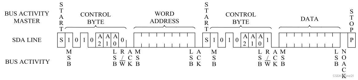
一次完整的传输包括 :起始位、停止位、控制字段、地址字段、读写数据字段
单字节地址写时序
 #### 双字节地址写时序

单字节地址读时序
双字节地址读时序

起始位
在时钟(SCL)为高电平的时候,数据总线(SDA)由高到低的跳变为总线 起始信号
停止位
在时钟(SCL)为高电平的时候,数据总线(SDA)由低到高的跳变为总线 停止信号
应答
应答,当数据发出方(不一定是主机还是从机)将 8 位数据或命令传出后,会将数据总线(SDA)释放,即设置为输入,然后等待数据接收方将 SDA 信号拉低以作为成功接收的应答信号。无论是什么状态,I2C 总线的 SCL 信号始终由 I2C 主机驱动。
RTL Code Design
代码参考了小梅哥的代码
1. 端口定义
module iic( clk, //系统时钟 rst_n, //系统复位 wr_en, //写使能 rd_en, //读使能 device_addr, //器件地址 reg_addr, //寄存器地址 reg_addr_num, //寄存器地址字节数 wr_data_num, //写数据字节数 rd_data_num, //读数据 sda, //IIC——SDA scl, //IIC——SCL wr_data, //写数据 rd_data, //读数据字节数 wr_data_vaild, //写数据有效 rd_data_vaild, //读数据有效 done //一次读写操作完成标志 ); /*端口定义*/ input clk; //系统时钟 input rst_n; //系统复位 input wr_en; //写使能 input rd_en; //读使能 input [2:0] device_addr; //器件地址 input [15:0] reg_addr; //寄存器地址 input [1:0] reg_addr_num; //寄存器地址字节数 input [5:0] wr_data_num; //写数据字节数 input [5:0] rd_data_num; //读数据 inout sda; //IIC——SDA output reg scl; //IIC——SCL input [7:0]wr_data; //写数据 output reg [7:0]rd_data; //读数据字节数 output wr_data_vaild; //读出数据有效 output reg rd_data_vaild; //写入数据有效 output reg done; //一次读写操作完成标志- 1
- 2
- 3
- 4
- 5
- 6
- 7
- 8
- 9
- 10
- 11
- 12
- 13
- 14
- 15
- 16
- 17
- 18
- 19
- 20
- 21
- 22
- 23
- 24
- 25
- 26
- 27
- 28
- 29
- 30
- 31
- 32
- 33
- 34
- 35
2. 参数定义
parameter SYS_CLOCK = 50_000_000; parameter SCL_CLOCK = 400_000; localparam SCL_CNT_M = SYS_CLOCK / SCL_CLOCK;- 1
- 2
- 3
3. 状态定义
localparam IDLE = 9'b0_0000_0001, WR_START = 9'b0_0000_0010, WR_CTRL = 9'b0_0000_0100, WR_REG_ADDR = 9'b0_0000_1000, WR_DATA = 9'b0_0001_0000, RD_START = 9'b0_0010_0000, RD_CTRL = 9'b0_0100_0000, RD_DATA = 9'b0_1000_0000, STOP = 9'b1_0000_0000;- 1
- 2
- 3
- 4
- 5
- 6
- 7
- 8
- 9
4. 内部寄存器和信号定义
reg [8:0]main_state; //状态寄存器 reg sda_reg; //sda输出寄存器 reg sda_en; //sda三态使能 reg sda_task_flag; //串行输出输入任务执行标志位 reg w_flag; //写标志 reg r_flag; //读标志 reg [15:0]scl_cnt; //clk计数器,用于产生scl时钟 reg scl_high; //scl高电平中部标志 reg scl_low; //scl低电平中部标志 reg scl_vaild; //scl有效标志 reg [7:0]scl_level_cnt;//scl高低电平计数器 reg ack; //应答信号 reg [7:0]wdata_cnt; //写数据字节数计数器 reg [7:0]rdata_cnt; //读数据字节数计数器 reg [1:0]reg_addr_cnt; //地址字节数计数器 reg [7:0]sda_data_out; //数据输出buffer reg [7:0]sda_data_in; //数据输入buffer wire [7:0]wr_ctrl_word; //写控制字 wire [7:0]rd_ctrl_word; //读控制字 wire rdata_vaild_r; //读数据有效前寄存器- 1
- 2
- 3
- 4
- 5
- 6
- 7
- 8
- 9
- 10
- 11
- 12
- 13
- 14
- 15
- 16
- 17
- 18
- 19
- 20
5. 读写控制字
assign wr_ctrl_word = {4'b1010,device_addr,1'b0}; assign rd_ctrl_word = {4'b1010,device_addr,1'b1};- 1
- 2
6.scl 时钟输出
/* iic 非空闲状态产生 scl_vaild */ always@(posedge clk or negedge rst_n)begin if(!rst_n) scl_vaild <= 1'b0; else if(wr_en | rd_en) scl_vaild <= 1'b1; else if(done) scl_vaild <= 1'b0; else scl_vaild <= scl_vaild; end /* scl 计数器*/ always@(posedge clk or negedge rst_n)begin if(!rst_n) scl_cnt <= 16'd0; else if(scl_vaild)begin if(scl_cnt==SCL_CNT_M-1) scl_cnt <= 16'd0; else scl_cnt <= scl_cnt + 16'd1; end else scl_cnt <= 16'd0; end /* scl 时钟产生*/ always@(posedge clk or negedge rst_n)begin if(!rst_n) scl <= 1'b1; else if(scl_cnt == SCL_CNT_M >> 1) scl <= 1'b0; else if(scl_cnt == 16'd0) scl <= 1'b1; else scl <= scl; end /*scl 高低电平中部标志*/ always@(posedge clk or negedge rst_n)begin if(!rst_n) scl_high <= 1'b0; else if(scl_cnt == (SCL_CNT_M >> 2)) scl_high <= 1'b1; else scl_high <= 1'b0; end always@(posedge clk or negedge rst_n)begin if(!rst_n) scl_low <= 1'b0; else if(scl_cnt == ((SCL_CNT_M >> 1) + (SCL_CNT_M >> 2))) scl_low <= 1'b1; else scl_low <= 1'b0; end- 1
- 2
- 3
- 4
- 5
- 6
- 7
- 8
- 9
- 10
- 11
- 12
- 13
- 14
- 15
- 16
- 17
- 18
- 19
- 20
- 21
- 22
- 23
- 24
- 25
- 26
- 27
- 28
- 29
- 30
- 31
- 32
- 33
- 34
- 35
- 36
- 37
- 38
- 39
- 40
- 41
- 42
- 43
- 44
- 45
- 46
- 47
- 48
- 49
- 50
- 51
- 52
- 53
- 54
- 55
- 56
7. 主状态机设计
always@(posedge clk or negedge rst_n)begin if(!rst_n)begin //复位:空闲状态 main_state <= IDLE; sda_reg <= 1'b1; w_flag <= 1'b0; r_flag <= 1'b0; done <= 1'b0; reg_addr_cnt <= 2'd1; wdata_cnt <= 8'd1; rdata_cnt <= 8'd1; end else begin case(main_state) IDLE:begin sda_reg <= 1'b1; w_flag <= 1'b0; r_flag <= 1'b0; done <= 1'b0; reg_addr_cnt <= 2'd1; wdata_cnt <= 8'd1; rdata_cnt <= 8'd1; if(wr_en)begin main_state <= WR_START; w_flag <= 1'b1; end else if(rd_en)begin main_state <= WR_START; r_flag <= 1'b1; end else main_state <= IDLE; end WR_START:begin if(scl_high)begin main_state <= WR_START; sda_reg <= 1'b0; end else if(scl_low)begin main_state <= WR_CTRL; sda_data_out <= wr_ctrl_word; // 准备要发送的控制字 sda_task_flag <= 1'b0; // 开始串行传输任务 end else main_state <= WR_START; end WR_CTRL:begin if(sda_task_flag==1'b0)// 发送数据 send_8bit_data; else begin // 等待响应 if(ack==1'b1)begin // 收到响应 if(scl_low)begin// 准备发送的寄存器地址数据 main_state <= WR_REG_ADDR;// 转换到寄存器地址 sda_task_flag <= 1'b0; if(reg_addr_num == 2'b1) sda_data_out <= reg_addr[7:0]; else sda_data_out <= reg_addr[15:8];//如果寄存器地址为2个字节,要保证先发的最高位 end else main_state <= WR_CTRL; end else // 未收到响应 main_state <= IDLE; end end WR_REG_ADDR:begin if(sda_task_flag==1'b0) send_8bit_data; else begin if(ack==1'b1)begin //收到响应 if(reg_addr_cnt == reg_addr_num)begin // 寄存器地址数据发送完成 if(w_flag && scl_low)begin main_state <= WR_DATA;//状态转移 sda_data_out <= wr_data;//数据准备 sda_task_flag <= 1'b0; reg_addr_cnt <= 2'd1; end else if(r_flag && scl_low)begin main_state <= RD_START; sda_reg <= 1'b1; //sda拉高 end else main_state <= WR_REG_ADDR; end else begin // 寄存器地址数据没有发送完成 if(scl_low)begin main_state <= WR_REG_ADDR; reg_addr_cnt <= reg_addr_cnt + 2'd1; sda_data_out <= reg_addr[7:0]; // 准备低8位寄存器地址 sda_task_flag <= 1'b0; end else main_state <= WR_REG_ADDR; end end else // 未收到响应 main_state <= IDLE; end end WR_DATA:begin if(sda_task_flag==1'b0) send_8bit_data; else begin if(ack==1'b1)begin// 收到响应 if(wdata_cnt == wr_data_num)begin //发送完成 if(scl_low)begin main_state <= STOP; sda_reg <= 1'b0; wdata_cnt <= 8'd1; end else main_state <= WR_DATA; end else begin //未发送完成 if(scl_low)begin main_state <= WR_DATA; sda_data_out <= wr_data; wdata_cnt <= wdata_cnt + 8'd1; sda_task_flag <= 1'b0; end else main_state <= WR_DATA; end end else // 未收到响应 main_state <= IDLE; end end RD_START:begin if(scl_high)begin main_state <= RD_START; sda_reg <= 1'b0; end else if(scl_low)begin main_state <= RD_CTRL; sda_data_out <= rd_ctrl_word; // 准备要发送的控制字 sda_task_flag <= 1'b0; // 开始串行传输任务 end else main_state <= RD_START; end RD_CTRL:begin if(sda_task_flag==1'b0)// 发送数据 send_8bit_data; else begin // 等待响应 if(ack==1'b1)begin // 收到响应 if(scl_low)begin// 准备发送的寄存器地址数据 main_state <= RD_DATA;// 转换到寄存器地址 sda_task_flag <= 1'b0; end else main_state <= RD_CTRL; end else // 未收到响应 main_state <= IDLE; end end RD_DATA:begin if(sda_task_flag==1'b0)begin receive_8bit_data; end else begin if(rdata_cnt==rd_data_num)begin// 接收完成 sda_reg <= 1'b1; //发送 ACK,不读了 if(scl_low)begin main_state <= STOP; sda_reg <= 1'b0; end else main_state <= RD_DATA; end else begin sda_reg <= 1'b0; // 发送NACK,继续读下一个字节 if(scl_low)begin main_state <= RD_DATA; rdata_cnt <= rdata_cnt + 8'd1; sda_task_flag <= 1'b0; end else main_state <= RD_DATA; end end end STOP:begin if(scl_high)begin sda_reg <= 1'b1; main_state <= IDLE; done <= 1'b1; end else main_state <= STOP; end default:main_state <= IDLE; endcase end end- 1
- 2
- 3
- 4
- 5
- 6
- 7
- 8
- 9
- 10
- 11
- 12
- 13
- 14
- 15
- 16
- 17
- 18
- 19
- 20
- 21
- 22
- 23
- 24
- 25
- 26
- 27
- 28
- 29
- 30
- 31
- 32
- 33
- 34
- 35
- 36
- 37
- 38
- 39
- 40
- 41
- 42
- 43
- 44
- 45
- 46
- 47
- 48
- 49
- 50
- 51
- 52
- 53
- 54
- 55
- 56
- 57
- 58
- 59
- 60
- 61
- 62
- 63
- 64
- 65
- 66
- 67
- 68
- 69
- 70
- 71
- 72
- 73
- 74
- 75
- 76
- 77
- 78
- 79
- 80
- 81
- 82
- 83
- 84
- 85
- 86
- 87
- 88
- 89
- 90
- 91
- 92
- 93
- 94
- 95
- 96
- 97
- 98
- 99
- 100
- 101
- 102
- 103
- 104
- 105
- 106
- 107
- 108
- 109
- 110
- 111
- 112
- 113
- 114
- 115
- 116
- 117
- 118
- 119
- 120
- 121
- 122
- 123
- 124
- 125
- 126
- 127
- 128
- 129
- 130
- 131
- 132
- 133
- 134
- 135
- 136
- 137
- 138
- 139
- 140
- 141
- 142
- 143
- 144
- 145
- 146
- 147
- 148
- 149
- 150
- 151
- 152
- 153
- 154
- 155
- 156
- 157
- 158
- 159
- 160
- 161
- 162
- 163
- 164
- 165
- 166
- 167
- 168
- 169
- 170
- 171
- 172
- 173
- 174
- 175
- 176
- 177
- 178
- 179
- 180
- 181
- 182
- 183
- 184
- 185
- 186
- 187
- 188
- 189
- 190
- 191
- 192
- 193
- 194
- 195
- 196
- 197
- 198
- 199
- 200
- 201
- 202
- 203
- 204
- 205
- 206
- 207
8. 发送接收任务
/* 发送接收8bit数据任务*/ /*发送接收数据时 scl 时钟计数*/ always@(posedge clk or negedge rst_n)begin if(!rst_n) scl_level_cnt <= 8'd0; else if(main_state == WR_CTRL || main_state == WR_REG_ADDR || main_state == WR_DATA || main_state == RD_CTRL || main_state == RD_DATA)begin //只有这几个状态需要执行数据发送接收任务 if(scl_low | scl_high)begin if(scl_level_cnt == 8'd17) scl_level_cnt <= 8'd0; else scl_level_cnt <= scl_level_cnt + 8'd1; end else scl_level_cnt <= scl_level_cnt; end else scl_level_cnt <= 8'd0; end /*数据接收对发送的响应标志位*/ always@(posedge clk or negedge rst_n)begin if(!rst_n) ack <= 1'b0; else if(scl_level_cnt == 8'd16 && scl_high && sda===1'd0) ack <= 1'b1; else if((scl_level_cnt == 8'd17)&& scl_low) ack <= 1'b0; else ack <= ack; end /* 输出串行数据任务 */ // scl_high & task send_8bit_data; if(scl_high && (scl_level_cnt == 8'd16))//8bit data send done sda_task_flag <= 1'b1; else if(scl_level_cnt < 8'd17)begin sda_reg <= sda_data_out[7]; if(scl_low) sda_data_out <= {sda_data_out[6:0],1'b0}; else sda_data_out <= sda_data_out; end else ; endtask /* 接收串行数据任务 */ // scl_high & scl_level_cnt==15 接收完成 // scl_low & scl_level_cnt==15 退出任务 task receive_8bit_data; if(scl_low && (scl_level_cnt==8'd15)) sda_task_flag <= 1'b1; else if(scl_level_cnt < 8'd15)begin if(scl_high) sda_data_in <= {sda_data_in[6:0],sda}; else sda_data_in <= sda_data_in; end else ; endtask- 1
- 2
- 3
- 4
- 5
- 6
- 7
- 8
- 9
- 10
- 11
- 12
- 13
- 14
- 15
- 16
- 17
- 18
- 19
- 20
- 21
- 22
- 23
- 24
- 25
- 26
- 27
- 28
- 29
- 30
- 31
- 32
- 33
- 34
- 35
- 36
- 37
- 38
- 39
- 40
- 41
- 42
- 43
- 44
- 45
- 46
- 47
- 48
- 49
- 50
- 51
- 52
- 53
- 54
- 55
- 56
- 57
- 58
- 59
- 60
- 61
- 62
- 63
- 64
9. sda 三态门输出控制
/*sda 三态门输出*/ assign sda = sda_en ? sda_reg : 1'bz; always@(*)begin case(main_state) IDLE: sda_en <= 1'b0;//输入 WR_START,RD_START,STOP : sda_en <= 1'b1;//输出 WR_CTRL,WR_REG_ADDR,WR_DATA,RD_CTRL: if(scl_level_cnt < 16) sda_en <= 1'b1; else sda_en <= 1'b0; RD_DATA: if(scl_level_cnt < 16) sda_en <= 1'b0; else sda_en <= 1'b1; default: sda_en <= 1'b0; endcase end- 1
- 2
- 3
- 4
- 5
- 6
- 7
- 8
- 9
- 10
- 11
- 12
- 13
- 14
- 15
- 16
- 17
- 18
- 19
- 20
- 21
- 22
- 23
- 24
- 25
- 26
10.读&写数据有效标志位
assign wr_data_vaild = ((main_state==WR_REG_ADDR)&& (reg_addr_cnt==reg_addr_num)&& (w_flag && scl_low)&& (ack == 1'b1))|| ((main_state == WR_DATA)&& (ack == 1'b1)&& (scl_low)&& (wdata_cnt != wr_data_num)); /*读出数据有效标志位*/ assign rdata_vaild_r = (main_state==RD_DATA) && (scl_level_cnt == 8'd15) && scl_low; always@(posedge clk or negedge rst_n)begin if(!rst_n) rd_data_vaild <= 1'b0; else if(rdata_vaild_r) rd_data_vaild <= 1'b1; else rd_data_vaild <= 1'b0; end- 1
- 2
- 3
- 4
- 5
- 6
- 7
- 8
- 9
- 10
- 11
- 12
- 13
- 14
- 15
- 16
- 17
- 18
11. 读出有效数据
/*读出的有效数据*/ always@(posedge clk or negedge rst_n)begin if(!rst_n) rd_data <= 8'd0; else if(rdata_vaild_r) rd_data <= sda_data_in; else rd_data <= rd_data; end- 1
- 2
- 3
- 4
- 5
- 6
- 7
- 8
- 9
12.仿真波形
24LC64.v
// ******************************************************************************************************* // ** ** // ** 24LC64.v - Microchip 24LC64 64K-BIT I2C SERIAL EEPROM (VCC = +2.5V TO +5.5V) ** // ** ** // ******************************************************************************************************* // ** ** // ** This information is distributed under license from Young Engineering. ** // ** COPYRIGHT (c) 2009 YOUNG ENGINEERING ** // ** ALL RIGHTS RESERVED ** // ** ** // ** ** // ** Young Engineering provides design expertise for the digital world ** // ** Started in 1990, Young Engineering offers products and services for your electronic design ** // ** project. We have the expertise in PCB, FPGA, ASIC, firmware, and software design. ** // ** From concept to prototype to production, we can help you. ** // ** ** // ** http://www.young-engineering.com/ ** // ** ** // ******************************************************************************************************* // ** This information is provided to you for your convenience and use with Microchip products only. ** // ** Microchip disclaims all liability arising from this information and its use. ** // ** ** // ** THIS INFORMATION IS PROVIDED "AS IS." MICROCHIP MAKES NO REPRESENTATION OR WARRANTIES OF ** // ** ANY KIND WHETHER EXPRESS OR IMPLIED, WRITTEN OR ORAL, STATUTORY OR OTHERWISE, RELATED TO ** // ** THE INFORMATION PROVIDED TO YOU, INCLUDING BUT NOT LIMITED TO ITS CONDITION, QUALITY, ** // ** PERFORMANCE, MERCHANTABILITY, NON-INFRINGEMENT, OR FITNESS FOR PURPOSE. ** // ** MICROCHIP IS NOT LIABLE, UNDER ANY CIRCUMSTANCES, FOR SPECIAL, INCIDENTAL OR CONSEQUENTIAL ** // ** DAMAGES, FOR ANY REASON WHATSOEVER. ** // ** ** // ** It is your responsibility to ensure that your application meets with your specifications. ** // ** ** // ******************************************************************************************************* // ** Revision : 1.4 ** // ** Modified Date : 02/04/2009 ** // ** Revision History: ** // ** ** // ** 10/01/2003: Initial design ** // ** 07/19/2004: Fixed the timing checks and the open-drain modeling for SDA. ** // ** 01/06/2006: Changed the legal information in the header ** // ** 12/04/2006: Corrected timing checks to reference proper clock edges ** // ** Added timing check for Tbuf (bus free time) ** // ** Reduced memory blocks to single, monolithic array ** // ** 02/04/2009: Added timing checks for tSU_WP and tHD_WP ** // ** ** // ******************************************************************************************************* // ** TABLE OF CONTENTS ** // ******************************************************************************************************* // **---------------------------------------------------------------------------------------------------** // ** DECLARATIONS ** // **---------------------------------------------------------------------------------------------------** // **---------------------------------------------------------------------------------------------------** // ** INITIALIZATION ** // **---------------------------------------------------------------------------------------------------** // **---------------------------------------------------------------------------------------------------** // ** CORE LOGIC ** // **---------------------------------------------------------------------------------------------------** // ** 1.01: START Bit Detection ** // ** 1.02: STOP Bit Detection ** // ** 1.03: Input Shift Register ** // ** 1.04: Input Bit Counter ** // ** 1.05: Control Byte Register ** // ** 1.06: Byte Address Register ** // ** 1.07: Write Data Buffer ** // ** 1.08: Acknowledge Generator ** // ** 1.09: Acknowledge Detect ** // ** 1.10: Write Cycle Timer ** // ** 1.11: Write Cycle Processor ** // ** 1.12: Read Data Multiplexor ** // ** 1.13: Read Data Processor ** // ** 1.14: SDA Data I/O Buffer ** // ** ** // **---------------------------------------------------------------------------------------------------** // ** DEBUG LOGIC ** // **---------------------------------------------------------------------------------------------------** // ** 2.01: Memory Data Bytes ** // ** 2.02: Write Data Buffer ** // ** ** // **---------------------------------------------------------------------------------------------------** // ** TIMING CHECKS ** // **---------------------------------------------------------------------------------------------------** // ** ** // ******************************************************************************************************* `timescale 1ns/10ps module M24LC64 (A0, A1, A2, WP, SDA, SCL, RESET); input A0; // chip select bit input A1; // chip select bit input A2; // chip select bit input WP; // write protect pin inout SDA; // serial data I/O input SCL; // serial data clock input RESET; // system reset // ******************************************************************************************************* // ** DECLARATIONS ** // ******************************************************************************************************* reg SDA_DO; // serial data - output reg SDA_OE; // serial data - output enable wire SDA_DriveEnable; // serial data output enable reg SDA_DriveEnableDlyd; // serial data output enable - delayed wire [02:00] ChipAddress; // hardwired chip address reg [03:00] BitCounter; // serial bit counter reg START_Rcvd; // START bit received flag reg STOP_Rcvd; // STOP bit received flag reg CTRL_Rcvd; // control byte received flag reg ADHI_Rcvd; // byte address hi received flag reg ADLO_Rcvd; // byte address lo received flag reg MACK_Rcvd; // master acknowledge received flag reg WrCycle; // memory write cycle reg RdCycle; // memory read cycle reg [07:00] ShiftRegister; // input data shift register reg [07:00] ControlByte; // control byte register wire RdWrBit; // read/write control bit reg [12:00] StartAddress; // memory access starting address reg [04:00] PageAddress; // memory page address reg [07:00] WrDataByte [0:31]; // memory write data buffer wire [07:00] RdDataByte; // memory read data reg [15:00] WrCounter; // write buffer counter reg [04:00] WrPointer; // write buffer pointer reg [12:00] RdPointer; // read address pointer reg WriteActive; // memory write cycle active reg [07:00] MemoryBlock [0:8191]; // EEPROM data memory array integer LoopIndex; // iterative loop index integer tAA; // timing parameter integer tWC; // timing parameter // ******************************************************************************************************* // ** INITIALIZATION ** // ******************************************************************************************************* //---------------------------- //------写数据间隔改动---------- initial tAA = 900; // SCL to SDA output delay initial tWC = 500; // memory write cycle time // initial tAA = 900; // SCL to SDA output delay // initial tWC = 5000000; // memory write cycle time initial begin SDA_DO = 0; SDA_OE = 0; end initial begin START_Rcvd = 0; STOP_Rcvd = 0; CTRL_Rcvd = 0; ADHI_Rcvd = 0; ADLO_Rcvd = 0; MACK_Rcvd = 0; end initial begin BitCounter = 0; ControlByte = 0; end initial begin WrCycle = 0; RdCycle = 0; WriteActive = 0; end assign ChipAddress = {A2,A1,A0}; // ******************************************************************************************************* // ** CORE LOGIC ** // ******************************************************************************************************* // ------------------------------------------------------------------------------------------------------- // 1.01: START Bit Detection // ------------------------------------------------------------------------------------------------------- always @(negedge SDA) begin if (SCL == 1) begin START_Rcvd <= 1; STOP_Rcvd <= 0; CTRL_Rcvd <= 0; ADHI_Rcvd <= 0; ADLO_Rcvd <= 0; MACK_Rcvd <= 0; WrCycle <= #1 0; RdCycle <= #1 0; BitCounter <= 0; end end // ------------------------------------------------------------------------------------------------------- // 1.02: STOP Bit Detection // ------------------------------------------------------------------------------------------------------- always @(posedge SDA) begin if (SCL == 1) begin START_Rcvd <= 0; STOP_Rcvd <= 1; CTRL_Rcvd <= 0; ADHI_Rcvd <= 0; ADLO_Rcvd <= 0; MACK_Rcvd <= 0; WrCycle <= #1 0; RdCycle <= #1 0; BitCounter <= 10; end end // ------------------------------------------------------------------------------------------------------- // 1.03: Input Shift Register // ------------------------------------------------------------------------------------------------------- always @(posedge SCL) begin ShiftRegister[00] <= SDA; ShiftRegister[01] <= ShiftRegister[00]; ShiftRegister[02] <= ShiftRegister[01]; ShiftRegister[03] <= ShiftRegister[02]; ShiftRegister[04] <= ShiftRegister[03]; ShiftRegister[05] <= ShiftRegister[04]; ShiftRegister[06] <= ShiftRegister[05]; ShiftRegister[07] <= ShiftRegister[06]; end // ------------------------------------------------------------------------------------------------------- // 1.04: Input Bit Counter // ------------------------------------------------------------------------------------------------------- always @(posedge SCL) begin if (BitCounter < 10) BitCounter <= BitCounter + 1; end // ------------------------------------------------------------------------------------------------------- // 1.05: Control Byte Register // ------------------------------------------------------------------------------------------------------- always @(negedge SCL) begin if (START_Rcvd & (BitCounter == 8)) begin if (!WriteActive & (ShiftRegister[07:01] == {4'b1010,ChipAddress[02:00]})) begin if (ShiftRegister[00] == 0) WrCycle <= 1; if (ShiftRegister[00] == 1) RdCycle <= 1; ControlByte <= ShiftRegister[07:00]; CTRL_Rcvd <= 1; end START_Rcvd <= 0; end end assign RdWrBit = ControlByte[00]; // ------------------------------------------------------------------------------------------------------- // 1.06: Byte Address Register // ------------------------------------------------------------------------------------------------------- always @(negedge SCL) begin if (CTRL_Rcvd & (BitCounter == 8)) begin if (RdWrBit == 0) begin StartAddress[12:08] <= ShiftRegister[04:00]; RdPointer[12:08] <= ShiftRegister[04:00]; ADHI_Rcvd <= 1; end WrCounter <= 0; WrPointer <= 0; CTRL_Rcvd <= 0; end end always @(negedge SCL) begin if (ADHI_Rcvd & (BitCounter == 8)) begin if (RdWrBit == 0) begin StartAddress[07:00] <= ShiftRegister[07:00]; RdPointer[07:00] <= ShiftRegister[07:00]; ADLO_Rcvd <= 1; end WrCounter <= 0; WrPointer <= 0; ADHI_Rcvd <= 0; end end // ------------------------------------------------------------------------------------------------------- // 1.07: Write Data Buffer // ------------------------------------------------------------------------------------------------------- always @(negedge SCL) begin if (ADLO_Rcvd & (BitCounter == 8)) begin if (RdWrBit == 0) begin WrDataByte[WrPointer] <= ShiftRegister[07:00]; WrCounter <= WrCounter + 1; WrPointer <= WrPointer + 1; end end end // ------------------------------------------------------------------------------------------------------- // 1.08: Acknowledge Generator // ------------------------------------------------------------------------------------------------------- always @(negedge SCL) begin if (!WriteActive) begin if (BitCounter == 8) begin if (WrCycle | (START_Rcvd & (ShiftRegister[07:01] == {4'b1010,ChipAddress[02:00]}))) begin SDA_DO <= 0; SDA_OE <= 1; end end if (BitCounter == 9) begin BitCounter <= 0; if (!RdCycle) begin SDA_DO <= 0; SDA_OE <= 0; end end end end // ------------------------------------------------------------------------------------------------------- // 1.09: Acknowledge Detect // ------------------------------------------------------------------------------------------------------- always @(posedge SCL) begin if (RdCycle & (BitCounter == 8)) begin if ((SDA == 0) & (SDA_OE == 0)) MACK_Rcvd <= 1; end end always @(negedge SCL) MACK_Rcvd <= 0; // ------------------------------------------------------------------------------------------------------- // 1.10: Write Cycle Timer // ------------------------------------------------------------------------------------------------------- always @(posedge STOP_Rcvd) begin if (WrCycle & (WP == 0) & (WrCounter > 0)) begin WriteActive = 1; #(tWC); WriteActive = 0; end end always @(posedge STOP_Rcvd) begin #(1.0); STOP_Rcvd = 0; end // ------------------------------------------------------------------------------------------------------- // 1.11: Write Cycle Processor // ------------------------------------------------------------------------------------------------------- always @(negedge WriteActive) begin for (LoopIndex = 0; LoopIndex < WrCounter; LoopIndex = LoopIndex + 1) begin PageAddress = StartAddress[04:00] + LoopIndex; MemoryBlock[{StartAddress[12:05],PageAddress[04:00]}] = WrDataByte[LoopIndex[04:00]]; end end // ------------------------------------------------------------------------------------------------------- // 1.12: Read Data Multiplexor // ------------------------------------------------------------------------------------------------------- always @(negedge SCL) begin if (BitCounter == 8) begin if (WrCycle & ADLO_Rcvd) begin RdPointer <= StartAddress + WrPointer + 1; end if (RdCycle) begin RdPointer <= RdPointer + 1; end end end assign RdDataByte = MemoryBlock[RdPointer[12:00]]; // ------------------------------------------------------------------------------------------------------- // 1.13: Read Data Processor // ------------------------------------------------------------------------------------------------------- always @(negedge SCL) begin if (RdCycle) begin if (BitCounter == 8) begin SDA_DO <= 0; SDA_OE <= 0; end else if (BitCounter == 9) begin SDA_DO <= RdDataByte[07]; if (MACK_Rcvd) SDA_OE <= 1; end else begin SDA_DO <= RdDataByte[7-BitCounter]; end end end // ------------------------------------------------------------------------------------------------------- // 1.14: SDA Data I/O Buffer // ------------------------------------------------------------------------------------------------------- bufif1 (SDA, 1'b0, SDA_DriveEnableDlyd); assign SDA_DriveEnable = !SDA_DO & SDA_OE; always @(SDA_DriveEnable) SDA_DriveEnableDlyd <= #(tAA) SDA_DriveEnable; // ******************************************************************************************************* // ** DEBUG LOGIC ** // ******************************************************************************************************* // ------------------------------------------------------------------------------------------------------- // 2.01: Memory Data Bytes // ------------------------------------------------------------------------------------------------------- wire [07:00] MemoryByte_000 = MemoryBlock[00]; wire [07:00] MemoryByte_001 = MemoryBlock[01]; wire [07:00] MemoryByte_002 = MemoryBlock[02]; wire [07:00] MemoryByte_003 = MemoryBlock[03]; wire [07:00] MemoryByte_004 = MemoryBlock[04]; wire [07:00] MemoryByte_005 = MemoryBlock[05]; wire [07:00] MemoryByte_006 = MemoryBlock[06]; wire [07:00] MemoryByte_007 = MemoryBlock[07]; wire [07:00] MemoryByte_008 = MemoryBlock[08]; wire [07:00] MemoryByte_009 = MemoryBlock[09]; wire [07:00] MemoryByte_00A = MemoryBlock[10]; wire [07:00] MemoryByte_00B = MemoryBlock[11]; wire [07:00] MemoryByte_00C = MemoryBlock[12]; wire [07:00] MemoryByte_00D = MemoryBlock[13]; wire [07:00] MemoryByte_00E = MemoryBlock[14]; wire [07:00] MemoryByte_00F = MemoryBlock[15]; // ------------------------------------------------------------------------------------------------------- // 2.02: Write Data Buffer // ------------------------------------------------------------------------------------------------------- wire [07:00] WriteData_00 = WrDataByte[00]; wire [07:00] WriteData_01 = WrDataByte[01]; wire [07:00] WriteData_02 = WrDataByte[02]; wire [07:00] WriteData_03 = WrDataByte[03]; wire [07:00] WriteData_04 = WrDataByte[04]; wire [07:00] WriteData_05 = WrDataByte[05]; wire [07:00] WriteData_06 = WrDataByte[06]; wire [07:00] WriteData_07 = WrDataByte[07]; wire [07:00] WriteData_08 = WrDataByte[08]; wire [07:00] WriteData_09 = WrDataByte[09]; wire [07:00] WriteData_0A = WrDataByte[10]; wire [07:00] WriteData_0B = WrDataByte[11]; wire [07:00] WriteData_0C = WrDataByte[12]; wire [07:00] WriteData_0D = WrDataByte[13]; wire [07:00] WriteData_0E = WrDataByte[14]; wire [07:00] WriteData_0F = WrDataByte[15]; wire [07:00] WriteData_10 = WrDataByte[16]; wire [07:00] WriteData_11 = WrDataByte[17]; wire [07:00] WriteData_12 = WrDataByte[18]; wire [07:00] WriteData_13 = WrDataByte[19]; wire [07:00] WriteData_14 = WrDataByte[20]; wire [07:00] WriteData_15 = WrDataByte[21]; wire [07:00] WriteData_16 = WrDataByte[22]; wire [07:00] WriteData_17 = WrDataByte[23]; wire [07:00] WriteData_18 = WrDataByte[24]; wire [07:00] WriteData_19 = WrDataByte[25]; wire [07:00] WriteData_1A = WrDataByte[26]; wire [07:00] WriteData_1B = WrDataByte[27]; wire [07:00] WriteData_1C = WrDataByte[28]; wire [07:00] WriteData_1D = WrDataByte[29]; wire [07:00] WriteData_1E = WrDataByte[30]; wire [07:00] WriteData_1F = WrDataByte[31]; // ******************************************************************************************************* // ** TIMING CHECKS ** // ******************************************************************************************************* wire TimingCheckEnable = (RESET == 0) & (SDA_OE == 0); wire StopTimingCheckEnable = TimingCheckEnable && SCL; //-------------------------------- //-------仿真时时序约束需改动-------- //-------------------------------- specify specparam tHI = 600, // SCL pulse width - high // tLO = 1300, // SCL pulse width - low tLO = 600, tSU_STA = 600, // SCL to SDA setup time tHD_STA = 600, // SCL to SDA hold time tSU_DAT = 100, // SDA to SCL setup time tSU_STO = 600, // SCL to SDA setup time tSU_WP = 600, // WP to SDA setup time tHD_WP = 1300, // WP to SDA hold time // tBUF = 1300; // Bus free time tBUF = 600; $width (posedge SCL, tHI); $width (negedge SCL, tLO); $width (posedge SDA &&& SCL, tBUF); $setup (posedge SCL, negedge SDA &&& TimingCheckEnable, tSU_STA); $setup (SDA, posedge SCL &&& TimingCheckEnable, tSU_DAT); $setup (posedge SCL, posedge SDA &&& TimingCheckEnable, tSU_STO); $setup (WP, posedge SDA &&& StopTimingCheckEnable, tSU_WP); $hold (negedge SDA &&& TimingCheckEnable, negedge SCL, tHD_STA); $hold (posedge SDA &&& StopTimingCheckEnable, WP, tHD_WP); endspecify endmodule- 1
- 2
- 3
- 4
- 5
- 6
- 7
- 8
- 9
- 10
- 11
- 12
- 13
- 14
- 15
- 16
- 17
- 18
- 19
- 20
- 21
- 22
- 23
- 24
- 25
- 26
- 27
- 28
- 29
- 30
- 31
- 32
- 33
- 34
- 35
- 36
- 37
- 38
- 39
- 40
- 41
- 42
- 43
- 44
- 45
- 46
- 47
- 48
- 49
- 50
- 51
- 52
- 53
- 54
- 55
- 56
- 57
- 58
- 59
- 60
- 61
- 62
- 63
- 64
- 65
- 66
- 67
- 68
- 69
- 70
- 71
- 72
- 73
- 74
- 75
- 76
- 77
- 78
- 79
- 80
- 81
- 82
- 83
- 84
- 85
- 86
- 87
- 88
- 89
- 90
- 91
- 92
- 93
- 94
- 95
- 96
- 97
- 98
- 99
- 100
- 101
- 102
- 103
- 104
- 105
- 106
- 107
- 108
- 109
- 110
- 111
- 112
- 113
- 114
- 115
- 116
- 117
- 118
- 119
- 120
- 121
- 122
- 123
- 124
- 125
- 126
- 127
- 128
- 129
- 130
- 131
- 132
- 133
- 134
- 135
- 136
- 137
- 138
- 139
- 140
- 141
- 142
- 143
- 144
- 145
- 146
- 147
- 148
- 149
- 150
- 151
- 152
- 153
- 154
- 155
- 156
- 157
- 158
- 159
- 160
- 161
- 162
- 163
- 164
- 165
- 166
- 167
- 168
- 169
- 170
- 171
- 172
- 173
- 174
- 175
- 176
- 177
- 178
- 179
- 180
- 181
- 182
- 183
- 184
- 185
- 186
- 187
- 188
- 189
- 190
- 191
- 192
- 193
- 194
- 195
- 196
- 197
- 198
- 199
- 200
- 201
- 202
- 203
- 204
- 205
- 206
- 207
- 208
- 209
- 210
- 211
- 212
- 213
- 214
- 215
- 216
- 217
- 218
- 219
- 220
- 221
- 222
- 223
- 224
- 225
- 226
- 227
- 228
- 229
- 230
- 231
- 232
- 233
- 234
- 235
- 236
- 237
- 238
- 239
- 240
- 241
- 242
- 243
- 244
- 245
- 246
- 247
- 248
- 249
- 250
- 251
- 252
- 253
- 254
- 255
- 256
- 257
- 258
- 259
- 260
- 261
- 262
- 263
- 264
- 265
- 266
- 267
- 268
- 269
- 270
- 271
- 272
- 273
- 274
- 275
- 276
- 277
- 278
- 279
- 280
- 281
- 282
- 283
- 284
- 285
- 286
- 287
- 288
- 289
- 290
- 291
- 292
- 293
- 294
- 295
- 296
- 297
- 298
- 299
- 300
- 301
- 302
- 303
- 304
- 305
- 306
- 307
- 308
- 309
- 310
- 311
- 312
- 313
- 314
- 315
- 316
- 317
- 318
- 319
- 320
- 321
- 322
- 323
- 324
- 325
- 326
- 327
- 328
- 329
- 330
- 331
- 332
- 333
- 334
- 335
- 336
- 337
- 338
- 339
- 340
- 341
- 342
- 343
- 344
- 345
- 346
- 347
- 348
- 349
- 350
- 351
- 352
- 353
- 354
- 355
- 356
- 357
- 358
- 359
- 360
- 361
- 362
- 363
- 364
- 365
- 366
- 367
- 368
- 369
- 370
- 371
- 372
- 373
- 374
- 375
- 376
- 377
- 378
- 379
- 380
- 381
- 382
- 383
- 384
- 385
- 386
- 387
- 388
- 389
- 390
- 391
- 392
- 393
- 394
- 395
- 396
- 397
- 398
- 399
- 400
- 401
- 402
- 403
- 404
- 405
- 406
- 407
- 408
- 409
- 410
- 411
- 412
- 413
- 414
- 415
- 416
- 417
- 418
- 419
- 420
- 421
- 422
- 423
- 424
- 425
- 426
- 427
- 428
- 429
- 430
- 431
- 432
- 433
- 434
- 435
- 436
- 437
- 438
- 439
- 440
- 441
- 442
- 443
- 444
- 445
- 446
- 447
- 448
- 449
- 450
- 451
- 452
- 453
- 454
- 455
- 456
- 457
- 458
- 459
- 460
- 461
- 462
- 463
- 464
- 465
- 466
- 467
- 468
- 469
- 470
- 471
- 472
- 473
- 474
- 475
- 476
- 477
- 478
- 479
- 480
- 481
- 482
- 483
- 484
- 485
- 486
- 487
- 488
- 489
- 490
- 491
- 492
- 493
- 494
- 495
- 496
- 497
- 498
- 499
- 500
- 501
- 502
- 503
- 504
- 505
- 506
- 507
- 508
- 509
- 510
- 511
- 512
- 513
- 514
- 515
- 516
- 517
- 518
- 519
- 520
- 521
- 522
- 523
- 524
- 525
- 526
- 527
- 528
- 529
- 530
- 531
- 532
- 533
- 534
- 535
- 536
- 537
- 538
- 539
- 540
- 541
- 542
- 543
- 544
- 545
24LC04B.v
// ******************************************************************************************************* // ** ** // ** 24LC04B.v - Microchip 24LC04B 4K-BIT I2C SERIAL EEPROM (VCC = +2.5V TO +5.5V) ** // ** ** // ******************************************************************************************************* // ** ** // ** This information is distributed under license from Young Engineering. ** // ** COPYRIGHT (c) 2003 YOUNG ENGINEERING ** // ** ALL RIGHTS RESERVED ** // ** ** // ** ** // ** Young Engineering provides design expertise for the digital world ** // ** Started in 1990, Young Engineering offers products and services for your electronic design ** // ** project. We have the expertise in PCB, FPGA, ASIC, firmware, and software design. ** // ** From concept to prototype to production, we can help you. ** // ** ** // ** http://www.young-engineering.com/ ** // ** ** // ******************************************************************************************************* // ** This information is provided to you for your convenience and use with Microchip products only. ** // ** Microchip disclaims all liability arising from this information and its use. ** // ** ** // ** THIS INFORMATION IS PROVIDED "AS IS." MICROCHIP MAKES NO REPRESENTATION OR WARRANTIES OF ** // ** ANY KIND WHETHER EXPRESS OR IMPLIED, WRITTEN OR ORAL, STATUTORY OR OTHERWISE, RELATED TO ** // ** THE INFORMATION PROVIDED TO YOU, INCLUDING BUT NOT LIMITED TO ITS CONDITION, QUALITY, ** // ** PERFORMANCE, MERCHANTABILITY, NON-INFRINGEMENT, OR FITNESS FOR PURPOSE. ** // ** MICROCHIP IS NOT LIABLE, UNDER ANY CIRCUMSTANCES, FOR SPECIAL, INCIDENTAL OR CONSEQUENTIAL ** // ** DAMAGES, FOR ANY REASON WHATSOEVER. ** // ** ** // ** It is your responsibility to ensure that your application meets with your specifications. ** // ** ** // ******************************************************************************************************* // ** Revision : 1.3 ** // ** Modified Date : 12/04/2006 ** // ** Revision History: ** // ** ** // ** 02/01/2003: Initial design ** // ** 07/19/2004: Fixed the timing checks and the open-drain modeling for SDA. ** // ** 01/06/2006: Changed the legal information in the header ** // ** 12/04/2006: Corrected timing checks to reference proper clock edges ** // ** Added timing check for Tbuf (bus free time) ** // ** ** // ******************************************************************************************************* // ** TABLE OF CONTENTS ** // ******************************************************************************************************* // **---------------------------------------------------------------------------------------------------** // ** DECLARATIONS ** // **---------------------------------------------------------------------------------------------------** // **---------------------------------------------------------------------------------------------------** // ** INITIALIZATION ** // **---------------------------------------------------------------------------------------------------** // **---------------------------------------------------------------------------------------------------** // ** CORE LOGIC ** // **---------------------------------------------------------------------------------------------------** // ** 1.01: START Bit Detection ** // ** 1.02: STOP Bit Detection ** // ** 1.03: Input Shift Register ** // ** 1.04: Input Bit Counter ** // ** 1.05: Control Byte Register ** // ** 1.06: Byte Address Register ** // ** 1.07: Write Data Buffer ** // ** 1.08: Acknowledge Generator ** // ** 1.09: Acknowledge Detect ** // ** 1.10: Write Cycle Timer ** // ** 1.11: Write Cycle Processor ** // ** 1.12: Read Data Multiplexor ** // ** 1.13: Read Data Processor ** // ** 1.14: SDA Data I/O Buffer ** // ** ** // **---------------------------------------------------------------------------------------------------** // ** DEBUG LOGIC ** // **---------------------------------------------------------------------------------------------------** // ** 2.01: Memory Data Bytes ** // ** 2.02: Write Data Buffer ** // ** ** // **---------------------------------------------------------------------------------------------------** // ** TIMING CHECKS ** // **---------------------------------------------------------------------------------------------------** // ** ** // ******************************************************************************************************* `timescale 1ns/10ps module M24LC04B (A0, A1, A2, WP, SDA, SCL, RESET); input A0; // unconnected pin input A1; // unconnected pin input A2; // unconnected pin input WP; // write protect pin inout SDA; // serial data I/O input SCL; // serial data clock input RESET; // system reset // ******************************************************************************************************* // ** DECLARATIONS ** // ******************************************************************************************************* reg SDA_DO; // serial data - output reg SDA_OE; // serial data - output enable wire SDA_DriveEnable; // serial data output enable reg SDA_DriveEnableDlyd; // serial data output enable - delayed reg [03:00] BitCounter; // serial bit counter reg START_Rcvd; // START bit received flag reg STOP_Rcvd; // STOP bit received flag reg CTRL_Rcvd; // control byte received flag reg ADDR_Rcvd; // byte address received flag reg MACK_Rcvd; // master acknowledge received flag reg WrCycle; // memory write cycle reg RdCycle; // memory read cycle reg [07:00] ShiftRegister; // input data shift register reg [07:00] ControlByte; // control byte register wire BlockSelect; // memory block select wire RdWrBit; // read/write control bit reg [08:00] StartAddress; // memory access starting address reg [03:00] PageAddress; // memory page address reg [07:00] WrDataByte [0:15]; // memory write data buffer wire [07:00] RdDataByte; // memory read data reg [15:00] WrCounter; // write buffer counter reg [03:00] WrPointer; // write buffer pointer reg [08:00] RdPointer; // read address pointer reg WriteActive; // memory write cycle active reg [07:00] MemoryBlock0 [0:255]; // EEPROM data memory array reg [07:00] MemoryBlock1 [0:255]; // EEPROM data memory array integer LoopIndex; // iterative loop index integer tAA; // timing parameter integer tWC; // timing parameter // ******************************************************************************************************* // ** INITIALIZATION ** // ******************************************************************************************************* //---------------------------- //------写数据间隔改动---------- initial tAA = 900; // SCL to SDA output delay initial tWC = 500; // memory write cycle time // initial tAA = 900; // SCL to SDA output delay // initial tWC = 5000000; // memory write cycle time initial begin SDA_DO = 0; SDA_OE = 0; end initial begin START_Rcvd = 0; STOP_Rcvd = 0; CTRL_Rcvd = 0; ADDR_Rcvd = 0; MACK_Rcvd = 0; end initial begin BitCounter = 0; ControlByte = 0; end initial begin WrCycle = 0; RdCycle = 0; WriteActive = 0; end // ******************************************************************************************************* // ** CORE LOGIC ** // ******************************************************************************************************* // ------------------------------------------------------------------------------------------------------- // 1.01: START Bit Detection // ------------------------------------------------------------------------------------------------------- always @(negedge SDA) begin if (SCL == 1) begin START_Rcvd <= 1; STOP_Rcvd <= 0; CTRL_Rcvd <= 0; ADDR_Rcvd <= 0; MACK_Rcvd <= 0; WrCycle <= #1 0; RdCycle <= #1 0; BitCounter <= 0; end end // ------------------------------------------------------------------------------------------------------- // 1.02: STOP Bit Detection // ------------------------------------------------------------------------------------------------------- always @(posedge SDA) begin if (SCL == 1) begin START_Rcvd <= 0; STOP_Rcvd <= 1; CTRL_Rcvd <= 0; ADDR_Rcvd <= 0; MACK_Rcvd <= 0; WrCycle <= #1 0; RdCycle <= #1 0; BitCounter <= 10; end end // ------------------------------------------------------------------------------------------------------- // 1.03: Input Shift Register // ------------------------------------------------------------------------------------------------------- always @(posedge SCL) begin ShiftRegister[00] <= SDA; ShiftRegister[01] <= ShiftRegister[00]; ShiftRegister[02] <= ShiftRegister[01]; ShiftRegister[03] <= ShiftRegister[02]; ShiftRegister[04] <= ShiftRegister[03]; ShiftRegister[05] <= ShiftRegister[04]; ShiftRegister[06] <= ShiftRegister[05]; ShiftRegister[07] <= ShiftRegister[06]; end // ------------------------------------------------------------------------------------------------------- // 1.04: Input Bit Counter // ------------------------------------------------------------------------------------------------------- always @(posedge SCL) begin if (BitCounter < 10) BitCounter <= BitCounter + 1; end // ------------------------------------------------------------------------------------------------------- // 1.05: Control Byte Register // ------------------------------------------------------------------------------------------------------- always @(negedge SCL) begin if (START_Rcvd & (BitCounter == 8)) begin if (!WriteActive & (ShiftRegister[07:04] == 4'b1010)) begin if (ShiftRegister[00] == 0) WrCycle <= 1; if (ShiftRegister[00] == 1) RdCycle <= 1; ControlByte <= ShiftRegister[07:00]; CTRL_Rcvd <= 1; end START_Rcvd <= 0; end end assign BlockSelect = ControlByte[01]; assign RdWrBit = ControlByte[00]; // ------------------------------------------------------------------------------------------------------- // 1.06: Byte Address Register // ------------------------------------------------------------------------------------------------------- always @(negedge SCL) begin if (CTRL_Rcvd & (BitCounter == 8)) begin if (RdWrBit == 0) begin StartAddress <= {BlockSelect,ShiftRegister[07:00]}; RdPointer <= {BlockSelect,ShiftRegister[07:00]}; ADDR_Rcvd <= 1; end WrCounter <= 0; WrPointer <= 0; CTRL_Rcvd <= 0; end end // ------------------------------------------------------------------------------------------------------- // 1.07: Write Data Buffer // ------------------------------------------------------------------------------------------------------- always @(negedge SCL) begin if (ADDR_Rcvd & (BitCounter == 8)) begin if ((WP == 0) & (RdWrBit == 0)) begin WrDataByte[WrPointer] <= ShiftRegister[07:00]; WrCounter <= WrCounter + 1; WrPointer <= WrPointer + 1; end end end // ------------------------------------------------------------------------------------------------------- // 1.08: Acknowledge Generator // ------------------------------------------------------------------------------------------------------- always @(negedge SCL) begin if (!WriteActive) begin if (BitCounter == 8) begin if (WrCycle | (START_Rcvd & (ShiftRegister[07:04] == 4'b1010))) begin SDA_DO <= 0; SDA_OE <= 1; end end if (BitCounter == 9) begin BitCounter <= 0; if (!RdCycle) begin SDA_DO <= 0; SDA_OE <= 0; end end end end // ------------------------------------------------------------------------------------------------------- // 1.09: Acknowledge Detect // ------------------------------------------------------------------------------------------------------- always @(posedge SCL) begin if (RdCycle & (BitCounter == 8)) begin if ((SDA == 0) & (SDA_OE == 0)) MACK_Rcvd <= 1; end end always @(negedge SCL) MACK_Rcvd <= 0; // ------------------------------------------------------------------------------------------------------- // 1.10: Write Cycle Timer // ------------------------------------------------------------------------------------------------------- always @(posedge STOP_Rcvd) begin if (WrCycle & (WP == 0) & (WrCounter > 0)) begin WriteActive = 1; #(tWC); WriteActive = 0; end end always @(posedge STOP_Rcvd) begin #(1.0); STOP_Rcvd = 0; end // ------------------------------------------------------------------------------------------------------- // 1.11: Write Cycle Processor // ------------------------------------------------------------------------------------------------------- always @(negedge WriteActive) begin for (LoopIndex = 0; LoopIndex < WrCounter; LoopIndex = LoopIndex + 1) begin if (StartAddress[08] == 0) begin PageAddress = StartAddress[03:00] + LoopIndex; MemoryBlock0[{StartAddress[07:04],PageAddress[03:00]}] = WrDataByte[LoopIndex[03:00]]; end if (StartAddress[08] == 1) begin PageAddress = StartAddress[03:00] + LoopIndex; MemoryBlock1[{StartAddress[07:04],PageAddress[03:00]}] = WrDataByte[LoopIndex[03:00]]; end end end // ------------------------------------------------------------------------------------------------------- // 1.12: Read Data Multiplexor // ------------------------------------------------------------------------------------------------------- always @(negedge SCL) begin if (BitCounter == 8) begin if (WrCycle & ADDR_Rcvd) begin RdPointer <= StartAddress + WrPointer + 1; end if (RdCycle) begin RdPointer <= RdPointer + 1; end end end assign RdDataByte = RdPointer[08] ? MemoryBlock1[RdPointer[07:00]] : MemoryBlock0[RdPointer[07:00]]; // ------------------------------------------------------------------------------------------------------- // 1.13: Read Data Processor // ------------------------------------------------------------------------------------------------------- always @(negedge SCL) begin if (RdCycle) begin if (BitCounter == 8) begin SDA_DO <= 0; SDA_OE <= 0; end else if (BitCounter == 9) begin SDA_DO <= RdDataByte[07]; if (MACK_Rcvd) SDA_OE <= 1; end else begin SDA_DO <= RdDataByte[7-BitCounter]; end end end // ------------------------------------------------------------------------------------------------------- // 1.14: SDA Data I/O Buffer // ------------------------------------------------------------------------------------------------------- bufif1 (SDA, 1'b0, SDA_DriveEnableDlyd); assign SDA_DriveEnable = !SDA_DO & SDA_OE; always @(SDA_DriveEnable) SDA_DriveEnableDlyd <= #(tAA) SDA_DriveEnable; // ******************************************************************************************************* // ** DEBUG LOGIC ** // ******************************************************************************************************* // ------------------------------------------------------------------------------------------------------- // 2.01: Memory Data Bytes // ------------------------------------------------------------------------------------------------------- wire [07:00] MemoryByte0_00 = MemoryBlock0[00]; wire [07:00] MemoryByte0_01 = MemoryBlock0[01]; wire [07:00] MemoryByte0_02 = MemoryBlock0[02]; wire [07:00] MemoryByte0_03 = MemoryBlock0[03]; wire [07:00] MemoryByte0_04 = MemoryBlock0[04]; wire [07:00] MemoryByte0_05 = MemoryBlock0[05]; wire [07:00] MemoryByte0_06 = MemoryBlock0[06]; wire [07:00] MemoryByte0_07 = MemoryBlock0[07]; wire [07:00] MemoryByte0_08 = MemoryBlock0[08]; wire [07:00] MemoryByte0_09 = MemoryBlock0[09]; wire [07:00] MemoryByte0_0A = MemoryBlock0[10]; wire [07:00] MemoryByte0_0B = MemoryBlock0[11]; wire [07:00] MemoryByte0_0C = MemoryBlock0[12]; wire [07:00] MemoryByte0_0D = MemoryBlock0[13]; wire [07:00] MemoryByte0_0E = MemoryBlock0[14]; wire [07:00] MemoryByte0_0F = MemoryBlock0[15]; wire [07:00] MemoryByte1_00 = MemoryBlock1[00]; wire [07:00] MemoryByte1_01 = MemoryBlock1[01]; wire [07:00] MemoryByte1_02 = MemoryBlock1[02]; wire [07:00] MemoryByte1_03 = MemoryBlock1[03]; wire [07:00] MemoryByte1_04 = MemoryBlock1[04]; wire [07:00] MemoryByte1_05 = MemoryBlock1[05]; wire [07:00] MemoryByte1_06 = MemoryBlock1[06]; wire [07:00] MemoryByte1_07 = MemoryBlock1[07]; wire [07:00] MemoryByte1_08 = MemoryBlock1[08]; wire [07:00] MemoryByte1_09 = MemoryBlock1[09]; wire [07:00] MemoryByte1_0A = MemoryBlock1[10]; wire [07:00] MemoryByte1_0B = MemoryBlock1[11]; wire [07:00] MemoryByte1_0C = MemoryBlock1[12]; wire [07:00] MemoryByte1_0D = MemoryBlock1[13]; wire [07:00] MemoryByte1_0E = MemoryBlock1[14]; wire [07:00] MemoryByte1_0F = MemoryBlock1[15]; // ------------------------------------------------------------------------------------------------------- // 2.02: Write Data Buffer // ------------------------------------------------------------------------------------------------------- wire [07:00] WriteData_0 = WrDataByte[00]; wire [07:00] WriteData_1 = WrDataByte[01]; wire [07:00] WriteData_2 = WrDataByte[02]; wire [07:00] WriteData_3 = WrDataByte[03]; wire [07:00] WriteData_4 = WrDataByte[04]; wire [07:00] WriteData_5 = WrDataByte[05]; wire [07:00] WriteData_6 = WrDataByte[06]; wire [07:00] WriteData_7 = WrDataByte[07]; wire [07:00] WriteData_8 = WrDataByte[08]; wire [07:00] WriteData_9 = WrDataByte[09]; wire [07:00] WriteData_A = WrDataByte[10]; wire [07:00] WriteData_B = WrDataByte[11]; wire [07:00] WriteData_C = WrDataByte[12]; wire [07:00] WriteData_D = WrDataByte[13]; wire [07:00] WriteData_E = WrDataByte[14]; wire [07:00] WriteData_F = WrDataByte[15]; // ******************************************************************************************************* // ** TIMING CHECKS ** // ******************************************************************************************************* wire TimingCheckEnable = (RESET == 0) & (SDA_OE == 0); //-------------------------------- //-------仿真时时序约束需改动-------- //-------------------------------- specify specparam tHI = 600, // SCL pulse width - high // tLO = 1300, // SCL pulse width - low tLO = 600, tSU_STA = 600, // SCL to SDA setup time tHD_STA = 600, // SCL to SDA hold time tSU_DAT = 100, // SDA to SCL setup time tSU_STO = 600, // SCL to SDA setup time // tBUF = 1300; // Bus free time tBUF = 600; $width (posedge SCL, tHI); $width (negedge SCL, tLO); $width (posedge SDA &&& SCL, tBUF); $setup (posedge SCL, negedge SDA &&& TimingCheckEnable, tSU_STA); $setup (SDA, posedge SCL &&& TimingCheckEnable, tSU_DAT); $setup (posedge SCL, posedge SDA &&& TimingCheckEnable, tSU_STO); $hold (negedge SDA &&& TimingCheckEnable, negedge SCL, tHD_STA); endspecify endmodule- 1
- 2
- 3
- 4
- 5
- 6
- 7
- 8
- 9
- 10
- 11
- 12
- 13
- 14
- 15
- 16
- 17
- 18
- 19
- 20
- 21
- 22
- 23
- 24
- 25
- 26
- 27
- 28
- 29
- 30
- 31
- 32
- 33
- 34
- 35
- 36
- 37
- 38
- 39
- 40
- 41
- 42
- 43
- 44
- 45
- 46
- 47
- 48
- 49
- 50
- 51
- 52
- 53
- 54
- 55
- 56
- 57
- 58
- 59
- 60
- 61
- 62
- 63
- 64
- 65
- 66
- 67
- 68
- 69
- 70
- 71
- 72
- 73
- 74
- 75
- 76
- 77
- 78
- 79
- 80
- 81
- 82
- 83
- 84
- 85
- 86
- 87
- 88
- 89
- 90
- 91
- 92
- 93
- 94
- 95
- 96
- 97
- 98
- 99
- 100
- 101
- 102
- 103
- 104
- 105
- 106
- 107
- 108
- 109
- 110
- 111
- 112
- 113
- 114
- 115
- 116
- 117
- 118
- 119
- 120
- 121
- 122
- 123
- 124
- 125
- 126
- 127
- 128
- 129
- 130
- 131
- 132
- 133
- 134
- 135
- 136
- 137
- 138
- 139
- 140
- 141
- 142
- 143
- 144
- 145
- 146
- 147
- 148
- 149
- 150
- 151
- 152
- 153
- 154
- 155
- 156
- 157
- 158
- 159
- 160
- 161
- 162
- 163
- 164
- 165
- 166
- 167
- 168
- 169
- 170
- 171
- 172
- 173
- 174
- 175
- 176
- 177
- 178
- 179
- 180
- 181
- 182
- 183
- 184
- 185
- 186
- 187
- 188
- 189
- 190
- 191
- 192
- 193
- 194
- 195
- 196
- 197
- 198
- 199
- 200
- 201
- 202
- 203
- 204
- 205
- 206
- 207
- 208
- 209
- 210
- 211
- 212
- 213
- 214
- 215
- 216
- 217
- 218
- 219
- 220
- 221
- 222
- 223
- 224
- 225
- 226
- 227
- 228
- 229
- 230
- 231
- 232
- 233
- 234
- 235
- 236
- 237
- 238
- 239
- 240
- 241
- 242
- 243
- 244
- 245
- 246
- 247
- 248
- 249
- 250
- 251
- 252
- 253
- 254
- 255
- 256
- 257
- 258
- 259
- 260
- 261
- 262
- 263
- 264
- 265
- 266
- 267
- 268
- 269
- 270
- 271
- 272
- 273
- 274
- 275
- 276
- 277
- 278
- 279
- 280
- 281
- 282
- 283
- 284
- 285
- 286
- 287
- 288
- 289
- 290
- 291
- 292
- 293
- 294
- 295
- 296
- 297
- 298
- 299
- 300
- 301
- 302
- 303
- 304
- 305
- 306
- 307
- 308
- 309
- 310
- 311
- 312
- 313
- 314
- 315
- 316
- 317
- 318
- 319
- 320
- 321
- 322
- 323
- 324
- 325
- 326
- 327
- 328
- 329
- 330
- 331
- 332
- 333
- 334
- 335
- 336
- 337
- 338
- 339
- 340
- 341
- 342
- 343
- 344
- 345
- 346
- 347
- 348
- 349
- 350
- 351
- 352
- 353
- 354
- 355
- 356
- 357
- 358
- 359
- 360
- 361
- 362
- 363
- 364
- 365
- 366
- 367
- 368
- 369
- 370
- 371
- 372
- 373
- 374
- 375
- 376
- 377
- 378
- 379
- 380
- 381
- 382
- 383
- 384
- 385
- 386
- 387
- 388
- 389
- 390
- 391
- 392
- 393
- 394
- 395
- 396
- 397
- 398
- 399
- 400
- 401
- 402
- 403
- 404
- 405
- 406
- 407
- 408
- 409
- 410
- 411
- 412
- 413
- 414
- 415
- 416
- 417
- 418
- 419
- 420
- 421
- 422
- 423
- 424
- 425
- 426
- 427
- 428
- 429
- 430
- 431
- 432
- 433
- 434
- 435
- 436
- 437
- 438
- 439
- 440
- 441
- 442
- 443
- 444
- 445
- 446
- 447
- 448
- 449
- 450
- 451
- 452
- 453
- 454
- 455
- 456
- 457
- 458
- 459
- 460
- 461
- 462
- 463
- 464
- 465
- 466
- 467
- 468
- 469
- 470
- 471
- 472
- 473
- 474
- 475
- 476
- 477
- 478
- 479
- 480
- 481
- 482
- 483
- 484
- 485
- 486
- 487
- 488
- 489
- 490
- 491
- 492
- 493
- 494
- 495
- 496
- 497
- 498
- 499
- 500
- 501
- 502
- 503
- 504
- 505
- 506
- 507
- 508
- 509
- 510
- 511
- 512
- 513
- 514
- 515
- 516
- 517
- 518
- 519
- 520
- 521
- 522
- 523
- 524
- 525
- 526
testbench
`timescale 1ns/1ns `define CLK_PERIOD 20 `define TEST_M24LC64 //24LC64 //`define TEST_M24LC04 //24LC04 module iic_tb; reg clk; reg rst_n; reg [15:0]reg_addr; reg [7:0]wr_data; wire [7:0]rd_data; reg rd_en; reg wr_en; wire rd_data_vaild; wire wr_data_vaild; wire sda; wire scl; wire done; localparam NUM = 6'd4; //单次读写数据字节数 `ifdef TEST_M24LC64 localparam DevAddr = 3'b000; //I2C 器件的器件地址 localparam WdAr_NUM= 2; //I2C 器件的存储器地址字节数 `elsif TEST_M24LC04 localparam DevAddr = 3'b001; //I2C 器件的器件地址 localparam WdAr_NUM= 1; //I2C 器件的存储器地址字节数 `endif iic iic( .clk(clk), //系统时钟 .rst_n(rst_n), //系统复位 .wr_en(wr_en), //写使能 .rd_en(rd_en), //读使能 .device_addr(DevAddr), //器件地址 .reg_addr(reg_addr), //寄存器地址 .reg_addr_num(WdAr_NUM), //寄存器地址字节数 .wr_data_num(NUM), //写数据字节数 .rd_data_num(NUM), //读数据 .sda(sda), //IIC——SDA .scl(scl), //IIC——SCL .wr_data(wr_data), //写数据 .rd_data(rd_data), //读数据字节数 .wr_data_vaild(wr_data_vaild), .rd_data_vaild(rd_data_vaild), .done(done) ); `ifdef TEST_M24LC64 M24LC64 M24LC64( .A0(1'b0), .A1(1'b0), .A2(1'b0), .WP(1'b0), .SDA(sda), .SCL(scl), .RESET(!rst_n) ); `elsif TEST_M24LC04 M24LC04B M24LC04( .A0(1'b1), .A1(1'b0), .A2(1'b0), .WP(1'b0), .SDA(sda), .SCL(scl), .RESET(!rst_n) ); `endif bufif1 (SDA, 1'b0, SDA_DriveEnableDlyd); initial clk = 1'b1; always #(`CLK_PERIOD/2)clk = ~clk; initial begin rst_n = 0; reg_addr = 0; wr_en = 0; wr_data = 0; rd_en = 0; #(`CLK_PERIOD*200 + 1) rst_n = 1; #200; `ifdef TEST_M24LC64 //仿真验证 24LC64 模型 //写入 20 组数据 reg_addr = 0; wr_data = 0; repeat(20)begin wr_en = 1'b1; #(`CLK_PERIOD); wr_en = 1'b0; repeat(NUM)begin //在写数据有效前给待写入数据 @(posedge wr_data_vaild) wr_data = wr_data + 1; end @(posedge done); #2000; reg_addr = reg_addr + NUM; end #2000; //读出刚写入的 20 组数据 reg_addr = 0; repeat(20)begin rd_en = 1'b1; #(`CLK_PERIOD); rd_en = 1'b0; @(posedge done); #2000; reg_addr = reg_addr + NUM; end `elsif TEST_M24LC04 //仿真验证 24LC04 模型 //写入 20 组数据 reg_addr = 100; wr_data = 100; repeat(20)begin wr_en = 1'b1; #(`CLK_PERIOD); wr_en = 1'b0; repeat(NUM)begin //在写数据有效前给待写入数据 @(posedge wr_data_vaild) wr_data = wr_data + 1; end @(posedge done); #2000; reg_addr = reg_addr + NUM; end #2000; //读出刚写入的 20 组数据 reg_addr = 100; repeat(20)begin rd_en = 1'b1; #(`CLK_PERIOD); rd_en = 1'b0; @(posedge done); #2000; reg_addr = reg_addr + NUM; end `endif #5000; $stop; end endmodule- 1
- 2
- 3
- 4
- 5
- 6
- 7
- 8
- 9
- 10
- 11
- 12
- 13
- 14
- 15
- 16
- 17
- 18
- 19
- 20
- 21
- 22
- 23
- 24
- 25
- 26
- 27
- 28
- 29
- 30
- 31
- 32
- 33
- 34
- 35
- 36
- 37
- 38
- 39
- 40
- 41
- 42
- 43
- 44
- 45
- 46
- 47
- 48
- 49
- 50
- 51
- 52
- 53
- 54
- 55
- 56
- 57
- 58
- 59
- 60
- 61
- 62
- 63
- 64
- 65
- 66
- 67
- 68
- 69
- 70
- 71
- 72
- 73
- 74
- 75
- 76
- 77
- 78
- 79
- 80
- 81
- 82
- 83
- 84
- 85
- 86
- 87
- 88
- 89
- 90
- 91
- 92
- 93
- 94
- 95
- 96
- 97
- 98
- 99
- 100
- 101
- 102
- 103
- 104
- 105
- 106
- 107
- 108
- 109
- 110
- 111
- 112
- 113
- 114
- 115
- 116
- 117
- 118
- 119
- 120
- 121
- 122
- 123
- 124
- 125
- 126
- 127
- 128
- 129
- 130
- 131
- 132
- 133
- 134
- 135
- 136
- 137
- 138
- 139
- 140
- 141
- 142
- 143
- 144
- 145
- 146
- 147
- 148
- 149
- 150
- 151
- 152
- 153
- 154
- 155
- 156
- 157
- 158
- 159
- 160
- 161
- 162
- 163
- 164
- 165
- 166
- 167
- 168
24LC04

24LC64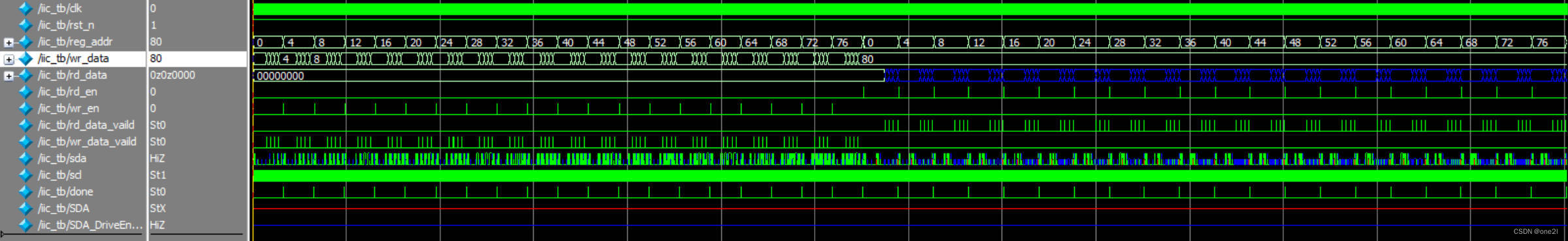
-
-
相关阅读:
OD机考真题:MELON的难题
速腾聚创发布全固态补盲激光雷达E1,成立合资公司,备战百万产能
图论| 827. 最大人工岛 127. 单词接龙
简单了解裸眼3D呈现技术
【已解决】Pyecharts折线图,只有坐标轴没有折线数据
35岁程序员炒Luna代币千万资产3天归零;俄罗斯调查谷歌等科技公司;Linux 5.19加入了50万行图形驱动代码|极客头条
荧光素酶报告基因
java中的IO缓冲流(高效流)---原始流的升级版
软件测试、交付与维护
Dubbo传输层及交换层实现
- 原文地址:https://blog.csdn.net/Rayone_/article/details/126818487
