-
深入理解计算机系统——第四章 Processor Architecture
深入理解计算机系统——第四章 Processor Architecture
- 4.1 The Y86-64 Instruction Set Architecture
- 4.2 Logic Design and the Hardware Control Language HCL
- 4.3 Sequential Y86-64 Implementations
- 4.4 General Principles of Pipelining
- 4.5 Pipelined Y86-64 Implementations
参考资源:
未仔细看
本章主要介绍处理器硬件的设计,并定义了一套简单的指令集 “Y86-64” ,便于学习。
In this chapter, we start by defining a simple instruction set that we use as a running example for our processor implementations. We call this the “Y86-64” instruction set, because it was inspired by the x86-64 instruction set.
Compared with x86-64, the Y86-64 instruction set has fewer data types, instructions, and addressing modes.4.1 The Y86-64 Instruction Set Architecture
We have seen that a processor must execute a sequence of instructions, where each instruction performs some primitive operation, such as adding two numbers.
An instruction is encoded in binary form as a sequence of 1 or more bytes. The instructions supported by a particular processor and their
byte-levelencodings are known as itsinstruction set architecture(ISA).Different “families” of processors, such as Intel
IA32andx86-64,IBM/Freescale Power, and theARMprocessor family, have differentISAs.A program compiled for one type of machine will not run on another.
On the other hand, there are many different models of processors within a single family.
Each manufacturer produces processors of ever-growing performance and complexity, but the different models remain compatible at the
ISAlevel.Defining an instruction set architecture, such as
Y86-64, includes defining the different components of its state, the set of instructions and their encodings, a set of programming conventions, and the handling of exceptional events.4.1.1 Programmer-Visible State
Each instruction in a
Y86-64program can read and modify some part of the processor state.This is referred to as the
programmer-visible state, where the “programmer” in this case is either someone writing programs in assembly code or a compiler generating machine-level code.There are 15 program registers:
%rax, %rcx, %rdx, %rbx, %rsp, %rbp, %rsi, %rdi, and %r8through %r14. (We omit thex86-64register%r15to simplify the instruction encoding.)Each of these stores a
64-bit word.Register
%rspis used as a stack pointer by the push, pop, call, and return instructions.Otherwise, the registers have no fixed meanings or values.
There are three single-bit condition codes,
ZF, SF, and OF, storing information about the effect of the most recent arithmetic or logical instruction.The program counter (PC) holds the address of the instruction currently being executed.
The memory is conceptually a large array of bytes, holding both program and data.
Y86-64programs reference memory locations usingvirtual addresses. A combination of hardware and operating system software translates these into the actual, or physical, addresses indicating where the values are actually stored in memory.A final part of the program state is a status code
Stat, indicating the overall state of program execution. It will indicate either normal operation or that some sort of exception has occurred, such as when an instruction attempts to read from an invalid memory address.见下图:

4.1.2 Y86-64 Instructions
-
The
x86-64movqinstruction is split into four different instructions:irmovq, rrmovq, mrmovq, and rmmovq, explicitly indicating the form of the source and destination. The source is either immediate (i), register (r), or memory(m). -
There are four integer operation instructions. These are
addq, subq, andq, and xorq. They operate only on register data, whereasx86-64also allows operations on memory data. These instructions set the three condition codesZF, SF, and OF(zero, sign, and overflow).

-
The seven jump instructions (shown in Figure 4.2 as
jXX) arejmp, jle, jl, je jne, jge, and jg. -
There are six conditional move instructions (shown in Figure 4.2 as
cmovXX):cmovle, cmovl, cmove, cmovne, cmovge, and cmovg. -
The
callinstruction pushes the return address on the stack and jumps to the destination address. Theretinstruction returns from such acall. -
The
pushq and popqinstructions implementpush and pop, just as they do inx86-64. -
The
haltinstruction stops instruction execution. ForY86-64, executing thehaltinstruction causes the processor to stop, with thestatus codeset toHLT.
4.1.3 Instruction Encoding
Each instruction requires between
1 and 10 bytes, depending on which fields are required.Every instruction has an initial byte identifying the
instruction type. This byte is split intotwo 4-bit parts: thehigh-order, orcode, part, and thelow-order, orfunction, part.
4.1.2 中图 4.2 所见第一个字节,高4位为指令代码(范围为0 - 0xB),低4位为指令功能。如halt的第一个字节,高四位和第四位都为0。The function values are significant only for the cases where a group of related instructions share a common code. These are given in Figure 4.3, showing the specific encodings of the integer operation, branch, and conditional move instructions.
低四位的部分只有当有一系列相关的有相同指令代码片段时才有意义,如MOV相关的指令rrmovl, cmovle, cmovl, cmove这四个指令第一个字节的高四位都为2,第四位不同。

As shown in Figure 4.4, each of the
15 program registershas an associatedregister identifier (ID)ranging from0 to 0xE.The numbering of registers in
Y86- 64matches what is used inx86-64. The program registers are stored within theCPUin aregister file, a smallrandom access memorywhere the register IDs serve as addresses.IDvalue0xFis used in the instruction encodings and within our hardware designs when we need to indicate that no register should be accessed.每个寄存器都有个
ID用来表示寄存器的类型,其中oxF表示没有寄存器。

从图 4.2 中可以看见,有些指令需要额外的寄存器,如rrmovq需要额外两个寄存器,一个存放源数据(rA),另一个存放目标数据(rB),而对于寄存器irmovq,由于源数据是立即数,无寄存器,因此第二个字节的高四位区域为0xF,表示无寄存器,低四位区域称为rB,该字节区域为register specifier byte。Some instructions require an additional 8-byte constant word. This word can serve as the immediate data for
irmovq, the displacement forrmmovqandmrmovqaddress specifiers, and thedestinationofbranchesandcalls.Note that
branchandcalldestinationsare given as absolute addresses, rather than using thePC-relative addressingseen inx86-64.As with
x86-64, all integers have a little-endian encoding.有些指令需要额外的 8 字节,如图 4.2 中指令
irmovq的第 3 ~ 10 个字节区域来存放立即数。示例:对于指令
rmmovq %rsp,0x123456789abcd(%rdx)(十六进制),根据图 4.2,第一个字节表示指令类型,值为40;第二个字节中,高四位
rA区域为源寄存器,即%rsp,从图 4.4 可以找到其 ID 为 4,而低4位rB区域为寄存器%rdx,其 ID 为 2,因此第二个字节为42;最后的 8 个字节区域存放常数
0x123456789abcd,将高位填充0,即为00 01 23 45 67 89 ab cd,写成小端序为cd ab 89 67 45 23 01。综上,最后得到该指令的二进制码为
4042cdab896745230100。4.1.4 Y86-64 Exceptions
图 4.1 中可知
programmer-visible state for Y86-64有个状态码Stat用来描述程序执行的状态,其可能的值如下图所示:

对于Y86-64, 设计当处理器遇到异常时停止执行。但在更复杂的设计中,处理器遇到异常时会 invoke an exception handler, a procedure designated to handle the specific type of exception encountered.
In a more complete design, the processor would typically invoke an exception handler, a procedure designated to handle the specific type of exception encountered.
4.2 Logic Design and the Hardware Control Language HCL
4.2.1 Logic Gates
逻辑门是数字电路中的基本计算元件:

4.2.2 Combinational Circuits and HCL Boolean Expressions
多个逻辑门组合起来构成一个组合电路,特点如下:
-
每个逻辑门的输入必须连到以下三种中的一种:
(1) one of the system inputs (known as a primary input), (2) the output
connection of some memory element, or (3) the output of some logic gate. -
多个逻辑门的输出不能连在一起。
-
The network must be acyclic. That is, there cannot be a path through a series of gates that forms a loop in the network. Such loops can cause ambiguity in the function computed by the network。
示例1:

上述组合电路实现的功能为:如果两个输入相等则输入 1,否则输出 0。
用HCL语言描述如下:bool eq = (a && b) || (!a && !b);- 1
Unlike C, however, we do not view this as performing a computation and assigning the result to some memory location. Instead, it is simply a way to give a name to an expression.
示例2 :

该组合电路实现的功能为single-bit多路复用器,s为控制信号,当s为1时,输出的结果为a,当s为0时,输出的结果为b。HCL语言描述为:bool out = (s && a) || (!s && b);- 1
注意
HCL语言和C语言区别:C 语言逻辑表达式可能只需要判断部分就能得出结论,那么剩下的表达式不会执行,而组合逻辑没有该规则,不会出现只判断部分。4.2.3 Word-Level Combinational Circuits and HCL Integer Expressions
Figure 4.12 shows a combinational circuit that tests whether two 64-bit words
AandBare equal.

对上图,如果
A的每个位都和B的相应的位相等,则A和B相等,输出位 1。In
HCL, we will declare any word-level signal as an int, without specifying the word size.图 4.12 可以表示为
bool Eq = (A == B);4.2.5 Memory and Clocking
Combinational circuits, by their very nature, do not store any information. Instead, they simply react to the signals at their inputs, generating outputs equal to some function of the inputs.To create sequential circuits—that is, systems that have state and perform computations on that state—we must introduce devices that store information represented as bits.
Our storage devices are all controlled by a single clock, a periodic signal that determines when new values are to be loaded into the devices.
We consider two classes of memory devices:
-
Clocked registers (or simply registers) store individual bits or words. The clock signal controls the loading of the register with the value at its input.
-
Random access memories (or simply memories) store multiple words, using an address to select which word should be read or written.
Examples of random access memories include (1) the virtual memory system of a processor, where a combination of hardware and operating system software make it appear to a processor that it can access any word within a large address space; and (2) the register file, where register identifiers serve as the addresses.
In a
Y86-64processor, the register file holds the 15 program registers (%raxthrough%r14).As we can see, the word “register” means two slightly different things when
speaking of hardware versus machine-language programming.In hardware, a register is directly connected to the rest of the circuit by its input and output wires.
In machine-level programming, the registers represent a small collection of addressable words in the
CPU, where the addresses consist of register IDs.Figure 4.16 gives a more detailed view of a hardware register and how it operates. For most of the time, the register remains in a fixed state (shown as x), generating an output equal to its current state.

见图 4.16 所示,对于硬件的寄存器,大多数时间会保持固定的状态(图中的 x),其输出即为当前的状态。
只要始终信号处于低电平(0),则寄存器的状态将保持不变。
当时钟信号处于高电平(1),寄存器的输入信号将传输到寄存器中更新其状态(y),因此其输出的结果更新为 y。Our
Y86-64 processorswill useclocked registersto hold theprogram counter (PC), thecondition codes (CC), and theprogram status (Stat).典型的寄存器文件如下:

This
register filehas two read ports, namedAandB, and one write port, namedW. Such a multiported random access memory allows multiple read and write operations to take place simultaneously.如果将
srcA的值设置为3,根据图 4.4,则会读寄存器%rbx,而该寄存器的值将会作为valA的结果输出。至于写输入到寄存器文件中,每次当时钟信号处于高电平时,输入到
valW接口的数据会写入接口dstW接口的数值(寄存器ID)所代表的寄存器中。如果dstW的职位oxF(无寄存器),则不会写入数据。如果寄存器文件同时读写同一个寄存器怎么处理?
As the clock rises, there will be a transition on the read port’s data output from the old value to the new.4.3 Sequential Y86-64 Implementations
As a first step, we describe a processor called
SEQ(for “sequential” processor). On each clock cycle,SEQperforms all the steps required to process a complete instruction.This would require a very long cycle time, however, and so the clock rate would be unacceptably low.
4.3.1 Organizing Processing into Stages
-
取指令(Fetch),根据程序计数器的值作为内存地址,从内存中读取指令。获取指令后,将提取指令的第一个字节(图 4.2 和 图4.3 中介绍),高4位位指定代码
icode,低四位为指令功能ifun,也可能根据需要用到后面字节的功能(见前面 4.1 节介绍),然后计算valP的值(程序计数器 PC的值 + 获取指令的长度)。 -
译码(Decode),The decode stage reads up to two operands from the register file, giving values
valA and/or valB. Typically, it reads the registers designated by instruction fieldsrA and rB, but for some instructions it reads register%rsp. -
执行(Excute),算数逻辑单元(ALU)根据指令(ifun 的值)执行操作,计算内存引用的有效地址,或者增加或减小栈指针。
-
访存(Memory),向内存中读或写数据,读的数据为
valM。 -
写回(Write back),将执行的结果写到寄存器文件中。
-
更新程序计数器(PC update),将程序计数器的值设置为下条指令的地址。
Figure 4.17 to illustrate the processing of different
Y86-64instructions.

为了简化硬件电路的复杂性,在设计时尽量更多的不同指令共享硬件。
For example, each of our processor designs containsa single arithmetic/logic unitthat is used in different ways depending on the type of instruction being executed.Figure 4.18 shows the processing required for instruction types
OPq(integer and logical operations),rrmovq(register-register move), andirmovq(immediateregister move).
图 4.8 展示了图 4.7 中指令的处理过程。

整数操作指令(
OPq rA, rB):- 取指令:根据 4.1.2 的内容可知,整型操作(
addq, subq, andq, and xorq)有相同的icodez(6),只需要两个字节,无常数,因此valP的值为PC + 2。 - 译码:读取两个操作数,分别将
rA和rB代表的寄存器的值分别赋给valA和valB。 - 执行:根据
ifun中代表的操作,对两个操作数执行计算,并将结果赋给valE,并设置条件码CC(ZF, SF, OF)。 - 写回:将结果
valE写道rB所代表的寄存器中。 - 更新程序计数器:将
valP的值赋给PC。
rrmovq指令:
取指令过程和上述整数操作相同,译码阶段,只需rA代表的寄存器中的值,执行时将valA的值加0作为结果,然后再写回时将结果赋给rB代表的寄存器,实现将一个寄存器的结果赋值给另一个寄存器。irmovq指令:
取指过程中增加常数存放区域,将常数赋值给valC,valP的值为PC + 10(多了 8 字节的常数区域)。 然后在执行的阶段直接将常速加0作为结果,在写回阶段将结果赋值给rB代表的寄存器,最后更新PC的值。rrmovq和mrmovq的操作过程如下:

和前面
rrmovq的区别是在访存阶段多了向内存中写入或者读数据的过程。注意
rmmovq和mrmovq的最后8个字节常量区域存放的内容为:displacement for rmmovq and mrmovq address specifiers
push和popq的操作过程如下:

和前面的区域之处是在译码阶段用到了栈指针
%rsp,执行阶段将栈指针的值减8(向下扩展栈空间,pushq)或者加8(向上缩减栈空间,弹出数据popq)。
控制转移指令
jumps, call, 和 ret:
跳转指令
jXX不需要register specifier byte(rrmovq指令第二个字节的内容),因此第二个字节存放常数;
在执行阶段,检查条件码CC和ifun中指令的功能来判断是否满足条件决定是否跳转,结果为1-bit的信号Cnd;最后在更新计数器阶段,如果Cnd为1,则跳转到valC处(跳转分支的位置),否则执行下一条指令valP。调用和返回指令 (
call和ret):
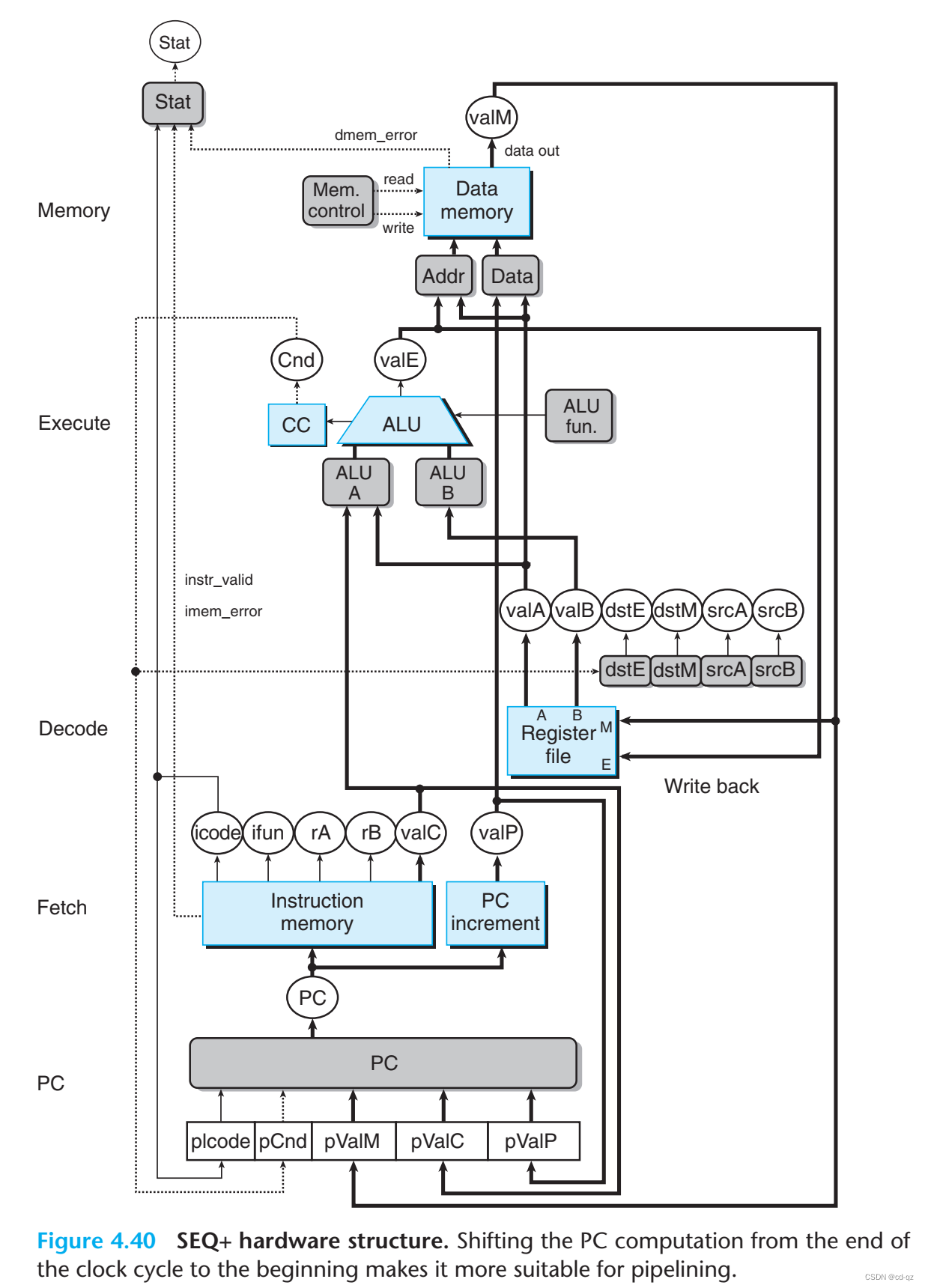
需要将下条要执行的指令地址压入或弹出栈。4.3.2 SEQ Hardware Structure
Abstract view of
SEQ, a sequential implementation:

In
SEQ, all of the processing by the hardware units occurs within a single clock cycle.上述流程图的操作过程是从下向上的过程。
Figure 4.23 gives a more detailed view of the hardware required to implement
SEQ.

4.3.3 SEQ Timing
Our implementation of
SEQconsists of combinational logic and two forms of memory devices:clocked registers(the program counter and condition code register) andrandom access memories(the register file, the instruction memory, and the data memory).The program counteris loaded with a new instruction address every clock cycle.The condition code registeris loaded only when aninteger operation instruction is executed.The data memoryis written only when anrmmovq, pushq, or call instruction is executed.The two write ports of the register fileallowtwo program registersto be updated on every cycle, but we can
use the special register ID0xFas a port address to indicate that no write should be performed for this port.principle: No reading back
The processor never needs to read back thestateupdated by an instruction in order to complete the processing of this instruction.The color coding in Figure 4.25 indicates how the circuit signals relate to the different instructions being executed.

4.3.4 SEQ Stage Implementations
HCL语言使用的常量:

-
Fetch Stage
取指令阶段:

-
Decode and Write-Back Stages
The register file has four ports. It supports up to two simultaneous reads (on ports A and B) and two simultaneous writes (on ports E and M).
这部分内容前面讲过。

-
Execute Stage
The execute stage includes the arithmetic/logic unit (ALU). This unit performs the operationadd, subtract, and, or exclusive-oron inputsaluA and aluBbased on the setting of thealufunsignal.

The hardware unit labeled “cond” uses a combination of the condition codes and the function code to determine whether a conditional branch or data transfer should take place (Figure 4.3). -
Memory Stage
The memory stage has the task of either reading or writing program data.

-
PC Update Stage
The final stage in SEQ generates the new value of the program counter (see Figure 4.31).

4.4 General Principles of Pipelining
A key feature of pipelining is that it increases the
throughputof the system (i.e., the number of customers served per unit time), but it may also slightly increase thelatency(i.e., the time required to service an individual customer).Figure 4.32(a) shows an example of a simple nonpipelined hardware system.

In this implementation, we must complete one instruction before beginning the next.
Three-stage pipelined computation hardware:


4.4.2 A Detailed Look at Pipeline Operation
Figure 4.35 traces the circuit activity between times 240 and 360, as instruction
I1(shown in dark gray) propagates through stageC,I2(shown in blue) propagates through stageB, andI3(shown in light gray) propagates through stageA.

As the clock rises and falls repeatedly, the different instructions flow through the stages of the pipeline without interfering with one another.
4.4.3 Limitations of Pipelining
Nonuniform Partitioning
图 4.35 所示的将操作过程分成三个阶段的方法有局限性:从一个阶段到下一个阶段之间会有延迟(50 - 150ps)。
However, the rate at which we can operate the clock is limited by the delay of the slowest stage.
以图 4.36 为例:

上图可看见每个阶段所用的时间不一致。
Devising a partitioning of the system computation into a series of stages having uniform delays can be a major challenge for hardware designers.
Often, some of the hardware units in a processor, such as the ALU and the memories, cannot be subdivided into multiple units with shorter delay.
Diminishing Returns of Deep Pipelining
图 4.37 所示将操作过程分成6个阶段,每个阶段 50ps,可以看见最小的始终周期缩短了。

存在问题:we do not get a doubling of the throughput, due to the delay through the pipeline registers.Modern processors employ very deep pipelines (15 or more stages) in an attempt to maximize the processor clock rate.
处理器将指令执行过程分成大量很小的步骤,因此每个步骤的延迟也很小。
4.4.4 Pipelining a System with Feedback
有些情况指令之间有依赖关系,如下图,第二条指令要用到第一条指令的数据:

这种有依赖关系的指令执行过程见下图:

4.5 Pipelined Y86-64 Implementations
本章介绍设计一个
pipelined Y86-64处理器。4.5.1 SEQ+: Rearranging the Computation Stages
首先做一个改变,将更新程序计数器的步骤从最后一步改到第一步(
SEQ+)。(后面 4.5.4 有讲这么做的目的)It is often used to balance the delays between the different stages of a pipelined system.
4.5.2 Inserting Pipeline Registers
在 SEQ+ 的不同阶段插入管道寄存器(pipeline regiesters)来设计
PIPE−处理器:

管道寄存器标签介绍:
-
F: holds apredictedvalue of the program counter. -
D: sits between thefetchanddecodestages. It holds information about the most recently fetched instruction for processing by thedecodestage. -
E: sits between thedecodeandexecutestages. It holds information about the most recently decoded instruction and the values read from theregister filefor processing by theexecutestage. -
M: sits between theexecuteandmemorystages. It holds the results of the most recently executed instruction for processing by the memory stage. It also holds information about branch conditions and branch targets for processing conditional jumps. -
W: sits between thememory stageand thefeedback pathsthat supply the computed results to theregister filefor writing and the return address to thePCselection logic when completing aretinstruction.
示例:

4.5.3 Rearranging and Relabeling Signals
对于不同阶段的状态码 (标签为
Stat),为了进行区分,加上前缀:D_stat, E_stat, M_stat, 和 W_stat。未看
4.5.4 Next PC Prediction
Our goal in the pipelined design is to issue a new instruction on every clock cycle, meaning that on each clock cycle, a new instruction proceeds into the execute stage and will ultimately be completed.
Achieving this goal would yield a throughput of one instruction per cycle.
To do this, we must determine the location of the next instruction right after fetching the current instruction.
但如果遇到条件分支或者
ret指令,将无法在取指令阶段知道下条指令的地址(见 4.3.1 节的图 4.21 说明)。因此,对于上述情况,需要预测程序计数器(PC)的下条指令的地址(3.6.3 节介绍跳转指令时提到过);该过程称为
分支预测(branch prediction)。4.5.5 Pipeline Hazards
如前面提到过,有时候指令之间有依赖关系,主要有两种:
(1)数据依赖
如下条指令需要用到本条指令的结果
(2)控制依赖
如跳转,调用指令和返回指令等,下条指令的地址由本条指令决定。如果依赖可能造成管道计算错误(预测错误),则称为 冒险(hazards)。
Like dependencies, hazards can be classified as either data hazards or control hazards.
示例1:

第一个示例可以正确得到结果,第一条指令在第
5个时钟周期向寄存器写入数据,第二条指令则在第6个时钟周期向寄存器写数据,而到第7个时钟周期addq指令才开始执行译码阶段,此时两个操作数均已更新。该示例能正确执行,因为加入了三个
nop指令在指令指令之间创建 延迟。示例2:

该示例相比示例1减少了一个
nop指令,在第6个时钟周期,指令2处于写回阶段,但写到寄存器中的数据要在下一个始终周期的开始(有高电平)时才更新数据,而此时addq指令已经处于译码阶段,因此计算错误。Avoiding Data Hazards by Stalling
One very general technique for avoiding hazards involves stalling, where the processor holds back one or more instructions in the pipeline until the hazard condition no longer holds.
例如示例2做如下修改:

在执行
addq指令前插入一个气泡 (bubble),在第7个时钟周期重复执行译码指令。A
bubbleis like a dynamically generatednopinstruction—it does not cause any changes to the registers, the memory, the condition codes, or the program status.这种方式的缺陷:
This will cause the pipeline to stall for up to three cycles, reducing the overall throughput significantlyAvoiding Data Hazards by Forwarding
示例2做如下修改:

根据前面的图 4.18 可知,在执行代码阶段,寄存器
%rax的值被写入到端口E(W_valE),因此正在第六个时钟周期执行addq的译码指令时,直接读取端口E的数据而非读取valB的数据。This technique of passing a result value directly from one pipeline stage to an earlier one is commonly known as
data forwarding(or simplyforwarding, and sometimesbypassing).Data forwarding requires adding additional data connections and control logic to the basic hardware structure.
下图 5.42 展示
PIPE的结构,能通过forwarding处理 hazards。

Load/Use Data Hazards
有一种情况不同哦通过
forwading的方式解决,如:
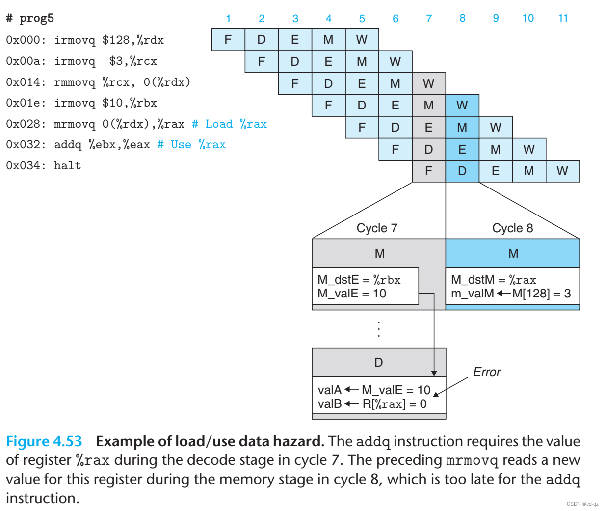
上图中,在7个时钟周期时,指令addq执行译码阶段,需要寄存器%rax的值,该值需要指令mrmovq在第8个时钟周期内存访问阶段才会得到(valM),因此无法使用forwarding的方法。图 4.54 展示一种使用
stalling和forwarding的组合方法:

上图在执行 `addq` 指令前插入一个气泡,因此在第7个时钟周期,`addq` 译码阶段能通过 `forwarding` 方式在`mrmovq` 的内存访问阶段获取数值。This use of a
stallto handle aload/use hazardis called aload interlock.Load interlockscombined withforwardingsuffice to handle all possible forms of data hazards.Avoiding Control Hazards
Control hazards arise when the processor cannot reliably determine the address of the next instruction based on the current instruction in the fetch stage.
Control hazards can only occur in our pipelined processor for
ret and jumpinstructions.示例:

上图中,指令2在译码阶段,进行分支预测,执行指令3,到四个时钟周期指令2到执行阶段才能判断分支预测是否正确,而此时已经错误的执行了指令3的两个阶段。
At this point, the pipeline can simply cancel (sometimes called instruction squashing) the two misfetched instructions by injecting bubbles into the decode and execute stages on the following cycle while also fetching the instruction following the jump instruction.
被错误执行的指令将从管道消失且不会对
programmer-visible state有任何影响。The only drawback is that two clock cycles’ worth of instruction processing capability have been wasted.
4.5.6 Exception Handling
内部异常:
(1) ahaltinstruction,
(2) an instruction with an invalid combination of instruction and function code
(3) an attempt to access an invalid address, either for instructionfetchordata read or write.In a pipelined system, exception handling involves several subtleties.
-
多个指令同时发生异常。
The basic rule is to put priority on the exception triggered by the instruction that is furthest along the pipeline.
In terms of the machine-language program, the instruction in the memory stage should appear to execute before one in the fetch stage, and therefore only this exception should be reported to the operating system. (?) -
在错误的分支预测中发生的异常,随后错误执行的指令会被取消。
The pipeline control logic will cancel this instruction, but we want to avoid raising an exception. -
A third subtlety arises because a pipelined processor updates different parts of the system state in different stages.
在同一个时钟周期,一个指令发生异常,而另一个指令使用异常指令的错误数据。
解决方案:使用状态码(`Stat``)
The exception status propagates through the pipeline with the rest of the information for that instruction, until it reaches the write-back stage.
At this point, the pipeline control logic detects the occurrence of the exception and stops execution.
To avoid having any updating of the
programmer-visible stateby instructions beyond the excepting instruction, the pipeline control logic must disable any updating of the condition code register or the data memory when an instruction in the memory or write-back stages has caused an exception.When an exception occurs in one or more stages of a pipeline, the information is simply stored in the status fields of the pipeline registers.
4.5.7 PIPE Stage Implementations
未细看
PIPEuses the same set of hardware units as the earlier sequential designs, with the addition of pipeline registers, some reconfigured logic blocks, and additional pipeline control logic.Many of the logic blocks are identical to their counterparts in
SEQandSEQ+, except that we must choose proper versions of the different signals from the pipeline registers (written with the pipeline register name, written in uppercase, as a prefix) or from the stage computations (written with the first character of the stage name, written in lowercase, as a prefix).示例:

They differ only in the prefixes added to the
PIPE signals:D_for the source values, to indicate that the signals come frompipeline register D, andd_for the result value, to indicate that it is generated in thedecode stage.
(4.5.2 和 4.5.3 节有讲)PC Selection and Fetch Stage
PIPEPCselection andfetchlogic:

ThePC selection logicchooses between three program counter sources.As a mispredicted branch enters the memory stage, the value of
valPfor this instruction (indicating the address of the following instruction) is read frompipeline register M (signal M_valA).When a
retinstruction enters thewrite-back stage, the return address is read from pipeline register W (signal W_valM).All other cases use the
predicted value of the PC, stored inpipeline register F (signal F_predPC):word f_pc = [ # Mispredicted branch. Fetch at incremented PC M_icode == IJXX && !M_Cnd : M_valA; # Completion of RET instruction W_icode == IRET : W_valM; # Default: Use predicted value of PC 1 : F_predPC; ];- 1
- 2
- 3
- 4
- 5
- 6
- 7
- 8
Unlike in
SEQ, we must split the computation of the instruction status into two parts.In the fetch stage, we can test for a memory error due to an out-of-range instruction address, and we can detect an illegal instruction or a
haltinstruction.Detecting an invalid data address must be deferred to the memory stage.
Decode and Write-Back Stages
Figure 4.58 gives a detailed view of the decode and write-back logic for PIPE.

Observe that the register IDs supplied to the write ports come from the
write-back stage(signals W_dstE and W_dstM`), rather than from the decode stage.This is because we want the writes to occur to the destination registers specified by the instruction in the write-back stage.
The block labeled “Sel+Fwd A” serves two roles.
It merges thevalPsignal into thevalAsignal for later stages in order to reduce the amount of state in the pipeline register.
It also implements theforwarding logicfor source operandvalA.There are
five different forwarding sources, each with a data word and a destinationregister ID:

If none of the forwarding conditions hold, the block should selectd_rvalA, the value read from registerport A, as its output.Putting all of this together, we get the following
HCLdescription for the new value ofvalAforpipeline register E:

The priority given to the five forwarding sources in the above
HCLcode is very important.The logic in the
HCLcode above first tests the forwarding source in the execute stage, then those in the memory stage, and finally the sources in the write-back stage.Execute Stage
Figure 4.60 shows the execute stage logic for
PIPE.

Memory Stage
Figure 4.61 shows the memory stage logic for
PIPE.

4.5.8 Pipeline Control Logic
This logic must handle the following four control cases for which other mechanisms, such as data forwarding and branch prediction, do not suffice:
- Load/use hazards. The pipeline must stall for one cycle between an instruction that reads a value from memory and an instruction that uses this value.
- Processing
ret. The pipeline must stall until theretinstruction reaches the write-back stage. - Mispredicted branches. By the time the branch logic detects that a jump should not have been taken, several instructions at the branch target will have started down the pipeline. These instructions must be canceled, and fetching should begin at the instruction following the jump instruction.
- Exceptions. When an instruction causes an exception, we want to disable the updating of the programmer-visible state by later instructions and
haltexecution once the excepting instruction reaches the write-back stage.
Pipeline Control Mechanisms
Figure 4.65 shows low-level mechanisms that allow the pipeline control logic to hold back an instruction in a pipeline register or to inject a bubble into the pipeline.

The table in Figure 4.66 shows the actions the different pipeline stages should take for each of the three special conditions.

Suppose that each pipeline register has two control inputs stall and bubble.
如图 4.5 所示,假设每个管道寄存器有两个控制输入stall和bubble。正常模式:两个输入均为0,在时钟信号变为高电平时,寄存器更新输入信号作为最新状态;
当
stall信号为1时,禁止更新状态,寄存器保持之前的状态;当
bubble信号为1时,the state of the register will be set to some fixed reset configuration, giving a state equivalent to that of anopinstruction. The particular pattern of ones and zeros for a pipeline register’s reset configuration depends on the set of fields in the pipeline register.Control Logic Implementation
Figure 4.68 shows the overall structure of the pipeline control logic.

4.5.9 Performance Analysis
A return instruction generates three bubbles, a load/use hazard generates one, and a mispredicted branch generates two.
We can quantify the effect these penalties have on the overall performance by computing an estimate of the average number of clock cycles
PIPEwould require per instruction it executes, a measure known
as theCPI(for “cycles per instruction”).If the stage processes a total of C i C_{i} Ci instructions and C b C_{b} Cb bubbles,


-
相关阅读:
工具-百度云盘服务-身份认证
每天一个数据分析题(四百)- 一元线性回归模型
在云上使用 OpenText 实现业务关键型应用程序的现代化
故障诊断 | GADF+Swin-CNN-GAM 的轴承故障诊断模型附matlab代码
Linux平台如何实现采集音视频数据并注入轻量级RTSP服务?
[M数学] lc2834. 找出美丽数组的最小和(数学+找规律+思维)
顺序容器
Flutter Don‘t use ‘BuildContext‘s across async gaps.
【单片机毕业设计】【mcuclub-hj-014】基于单片机的工地降尘的设计
远程发送剪切板,屏幕截图
- 原文地址:https://blog.csdn.net/Lee567/article/details/126172208