-
如何缩减layout电路面积?减少晶体管的数量——以全加器为例【VLSI】
如何缩减layout电路面积?减少晶体管的数量——以全加器为例【VLSI】
前言:
How to reduce the number of transistors to reduce circuit area? – Take the Binary Full Adder as an example优化面积的方法
- 减少晶体管的数量
- 改变gate matrix的布局
What is Full adder ?
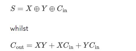
A full adder adds binary numbers and accounts for values carried in as well as out. A one-bit full-adder adds three one-bit numbers, often written as A, B, and Cin; A and B are the operands, and Cin is a bit carried in from the previous less-significant stage.

- 全加器的真值表:
Inputs Outputs A B Cin Cout S 0 0 0 0 0 0 0 1 0 1 0 1 0 0 1 0 1 1 1 0 1 0 0 0 1 1 0 1 1 0 1 1 0 1 0 1 1 1 1 1 全加器的设计方法
1. 32T 原始表达式不经过化简的电路图
根据真值表直接写表达式
根据表达式直接画晶体管图
在上图中,一个全加器有32个晶体管(6 for inverters,10 for the majority gate 进位,16 for the 3-input XOR gate)2. 28个晶体管 最基本的静态互补CMOS电路的全加器
静态互补CMOS
A static complementary CMOS gate is a combination of two networks, called the pull-up network (PUN) and the pull-down network (PDN).

静态互补CMOS的优势与劣势
- Advantages of static CMOS
- Low static power
- Robust
- Supported by most synthesis & back-end tools
- “Disadvantages” of static CMOS
- For N inputs, requires (at least) 2N transistors
- PUN can be area consuming
- Same function is computed twice
28T 电路图
利用逻辑方程直接转变成CMOS电路,进行逻辑变换。
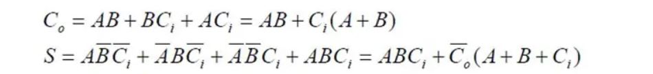

可以看到:
-
上图的逻辑,静态互补电路输出的Cout和S符合逻辑表达式。
-
输出Cout和S上,有一个反相器,两个晶体管的栅极连接在一起。我一开始很迷惑为什么需要加反相器,其实是因为静态互补CMOS这种设计方法,比如上图中的Cout表达式,实际是PDN的电路,PUN是取反之后的。为了让Cout为1,需要X为0,需要PDN下拉网络的A*B+Cin(A+B)起作用。反相器不能省,也可以防止噪音。
28T的棒状图Stick Diagram
稍微平移一下也可以画成这样

3. 24个晶体管 镜像CMOS加法器(mirror full adder)设计
怎么实现的镜像电路?
简单点说:移除输出反相器并交替正负逻辑以将延迟和晶体管数量减少到 24个。拿掉输出端的反相器并不影响电路的功能。拿掉输出端的反相器后形成了像镜像一样的NMOS和PMOS网络。
- Mirror adder : remove the output inverters and alternate positive and negative logic to reduce delay and transistor count to 24. The PMOS network is identical to the NMOS network rather than being the conduction complement.
原理的理解如下
-
观察到输出Cout端、S端的反相器

-
第二步理解,全加器是将低位进位输入也代入计算的加法电路,同样输出一个结果位和进位。全加器进位的链接是通过反相器来保证逻辑一致,Carry chain optimisation: using inversion property

-
如果去掉反相器会发生什么?输出端的Cin和S都会取反。那么怎么在去掉反相器的前提下保证输出端的Cin和S正常输出不会取反呢?——通过取反输入逻辑可以实现!即将“反相单元”从输出端移动到输入端。
-
如果将“反相单元”从输出端移动到输入端,则可以简化许多电路。不需要让每一级都包含一个反相器,以便其输入和输出具有相同的逻辑极性,当在乎的是面积损耗的时候,允许完全消除这些反相器。

-
取消了进位反相门,门的PDN和PUN不再是对偶网络,而是巧妙地实现了进位传播/产生/取消功能——当D或者G为高时,(~ Cout)分别被置为VDD或GND。当满足进位条件(P为1时),输入进位(以反相地形式)传播到(~ Cout)。
-
这些直接对应于电路的上拉结构,只需要将输出反转即可获得所需的结果。
总结:This simplification reduces the number of series transistors and makes the layout more uniform. If you invert your carrychain after each fulladder, you can spare the NOT gate and use an NOR gate -> 2 transistors.
理解: Carry Propagation
理解Carry Propagation这个进位过程是怎么实现的
用P(进位传播)、G(进位产生)、D-Kill(进位消除)表示全加器进位这个传播过程。

- Generate function: The generate signal G occurs when a C output is generated internally within the adder. G = A . B
- Propagate function: When the propagate signal P is true then Cin is passed to C when Cin is true. P = A + B; but we can also use P = A ⨁ \bigoplus ⨁(异或)B since it shows the same behaviour and also can be used to generate the sum term.

24T Mirror full adder 电路图
公式推导见上上上个图片。

24T 的棒状图Stick Diagram - Mirror full adder

注:这里的输出是 ~Cout 和 ~Sum ,如果需要得到正的输出Cout和Sum,需要加两个反相器,一共28个transistors。
这样的设计可以平衡PUN和PDN的结构,像对称镜像一样。

4. 24个晶体管 TG传输晶体管逻辑门Transmission Gate
传输门TG用于实现电子开关和模拟多路复用器。它通过消除冗余晶体管减少了用于制造不同逻辑门的晶体管数量。最大的特点是它的和与进位输出具有相似的延时。传输晶体管传输门逻辑的使用比互补 CMOS 更节能。
Logic circuits can be constructed with the aid of transmission gates instead of traditional CMOS pull-up and pull-down networks. Such circuits can often be made more compact, which can be an important consideration in silicon implementations.传输晶体管逻辑门(Transmission Gate)
A transmission gate is an electronic element and good non mechanical relay built with CMOS technology. It is made by parallel combination of nMOS and pMOS transistors with the input at the gate of one transistor © being complementary to the input at the gate of the other.
NMOS的Source端和PMOS的Source端连接到输入端,NMOS的Drain端和PMOS的Drain端连接到输出端。

Transmission Gate as a CMOS Bilateral Switch
- 什么是CMOS Switch?
MOS管技术使用 NMOS 和 PMOS 器件来执行逻辑开关功能,从而允许数字计算机或逻辑电路控制这些模拟开关的操作。NMOS 和 PMOS 晶体管都被制造到同一个门电路中的 CMOS 器件可以通过(关闭条件)或阻止(打开条件)模拟或数字信号,具体取决于控制它的数字逻辑电平。 - 什么是TG双向开关?
允许双向信号或数据传输的固态开关类型称为传输门或TG。 - 它将选择性地阻止或传递从输入到输出的信号电平。
When control signal C is high i.e. VDD, both transistor are on and provides a low resistance path between A and B. On the other hand, when C is low both are turned off and provide high impedance path between A and B.
TG的棒状图Stick Diagram

TG传输门用来构建XOR电路
The XOR gate can also be implemented by the use of Transmission gates with pass transistor logic.
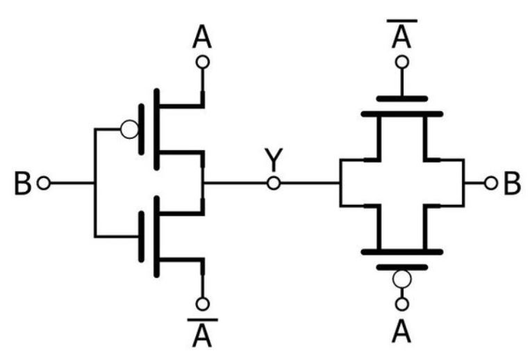
分析TG传输门构建的XOR电路:- 把上图看作两部分:左边是一个特殊的反相器,不过他的正电压是由A控制,负电压是由 A ‾ \overline{A} A控制。右边是一个传输门构成的CMOS开关,TG传输门的开关由 A ‾ \overline{A} A控制:当 A ‾ \overline{A} A为1的时候传输门打开。
- 当A为1时:先看右半面,由于 A ‾ \overline{A} A = 0 所以传输门关闭,不管B输入什么输出都为高阻态;左半面表现为一个标准的 CMOS 反相器 (其中 A 是 VCC, A ‾ \overline{A} A是GND)。所以我们可以推断出Y= B ‾ \overline{B} B。
- 当A为0时:先看右半面,由于 A ‾ \overline{A} A = 1 所以传输门打开,可以推断出Y=B;再看左半面,反相器的PMOS部分接的GND,NMOS部分接的VDD,所以两个MOS管都偏置关闭了,反相器一直均不工作。
XOR真值表对应
Input Output A B A XOR B 0 0 0 0 1 1 1 0 1 1 1 0 如果我想只用电线和晶体管构建一个逻辑异或门,我必须使用的最少数量的晶体管是多少?
对比CMOS静态互补电路组成的XOR电路(第一个图和第二个图都有22个MOS管),TG传输门构建的XOR电路共用了4个MOS管,共节省了18个MOS管。
2-input AND有6个MOS,2-input OR 有6个MOS,反相器有2个。

TG传输门实现 2:1 多路复用器
24T TG 全加器
按照全加器的逻辑表达式,将其改成含XOR异或门的表达式。

化简过程讲解Full Adder using Transmission Gates (Part 1) | transmission gate logic
uses Transmission Gate to form multiplexers and XORs. using 24 transistors and providing buffered outputs of the proper polarity with equal delay.

5.6个晶体管的 PTL传输晶体管逻辑 Pass Transistor Logic
Pass Transistor Logic 传输晶体管逻辑
这个PPT里写的Pass Transistor Circuit,一样的意思。

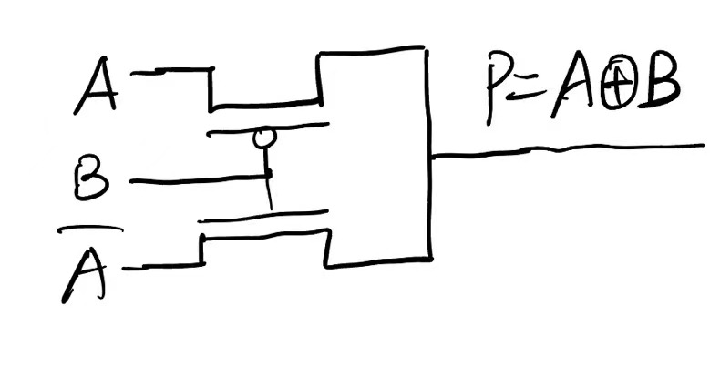
PTC实现XOR逻辑只需要2个MOS管

分析:将上图分为左右两个部分
- 当B为1时,先看左半部分, B ‾ \overline{B} B = 0 ,所以左半部分一直输出高阻态。再看右半部分,B = 1,所以右半部分输出随输入 A ‾ \overline{A} A 而正比变化。当A=1时, A ‾ \overline{A} A=0,F为0、当A =0时, A ‾ \overline{A} A=1,F为1。
- 当B为0时,先看左半部分,
B
‾
\overline{B}
B = 1 ,所以左半部分输出随输入A而正比变化。再看右半部分,B = 0,所以右半部分一直输出高阻态。当A=1时,F为1,当A =0时,F为0。
再把上图简化一下,因为输入带着负号
全加器的pass transistor 简化过程

6T 的电路图

6T IMPLEMENTATION AND ANALYSIS OF 6T 1BIT FULL ADDER USING CADENCE VIRTUOSO
Reference
Lecture 14: Pass transistors and transmission gates
EE141-Fall 2010 Fall 2010 Digital Integrated Digital Integrated Circuits
镜像 CMOS Static & Dynamic Logic Gates
Comparative Analysis of Different Types of Full Adder Circuits不同类型全加器电路的比较分析
Harvey Mudd College- Introduction to CMOS VLSI Design-adders
Please help me understand how this cmos mirror adder works
1bit Full Adder Cell in IC not working as supposed?
14 TRANSISTOR FULL ADDER CIRCUIT USING 4 TRANSISTOR XOR GATE AND TRANSMISSION GATE
CMOS Static & Dynamic Logic Gates
Power and Delay Comparison in between Different types of Full Adder Circuits
-
相关阅读:
函数的凹凸性与拐点
mysql数据文件
java 遍历文件夹目录树形结构并在控制台输出且保存到本地文件
JavaScript之观察者模式
如何将webp格式转换成png
如何设计一个可扩展的登录功能
内网穿透的应用-通过内网穿透快速搭建公网可访问的Spring Boot接口调试环境
[附源码]计算机毕业设计校园代取快递系统Springboot程序
数据结构——图结构
【剑指Offer】:循环有序列表的插入(涉及链表的知识)
- 原文地址:https://blog.csdn.net/qq_43858116/article/details/127957134